PD3536 OSRAM Opto Semiconductors Inc, PD3536 Datasheet - Page 12
PD3536
Manufacturer Part Number
PD3536
Description
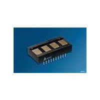
DISPLAY PROGR 4CHAR .27" RED
Manufacturer
OSRAM Opto Semiconductors Inc
Series
Alphanumeric Programmable Display™r
Datasheet
1.PD3535.pdf
(14 pages)
Specifications of PD3536
Millicandela Rating
30µcd
Size / Dimension
1.40" L x 0.72" W x 0.29" H (35.56mm x 18.29mm x 7.24mm)
Color
Red
Configuration
5 x 7
Number Of Digits
4
Character Size
0.27 in
Illumination Color
Red
Wavelength
660 nm
Maximum Operating Temperature
+ 85 C
Minimum Operating Temperature
- 40 C
Luminous Intensity
30 ucd
Viewing Area (w X H)
6.86 mm x 5.08 mm
Display Type
5 x 7 Dot Matrix
Lead Free Status / RoHS Status
Lead free / RoHS Compliant
Voltage - Forward (vf) Typ
-
Internal Connection
-
Lead Free Status / Rohs Status
Details
Other names
Q68000A8365


Electrical and Mechanical Considerations
The CMOS IC of the display is designed to provide resistance to
both Electrostatic Discharge Damage and Latch Up due to voltage
or current surges. Several precautions are strongly recommended
to avoid overstressing these built-in safeguards.
ESD Protection
Display users should be careful to handle the devices consistent
with Standard ESD protection procedures. Operators should wear
appropriate wrist, ankle or feet ground straps and avoid clothing
that collects static charges. Work surfaces, tools and transport car-
riers that come into contact with unshielded devices or assemblies
should also be appropriately grounded.
Latch up Protection
Latch up is a condition that occurs in CMOS ICs after the input
protection diodes have been broken down. These diodes can be
reversed through several means:
V
on the inputs. When these situations exist, the IC may develop the
response of an SCR and begin conducting as much as one amp
through the V
until device failure or the device is turned off.
The Voltage Transient Suppression Techniques and buffer inter-
faces for longer cable runs help considerably to prevent latch con-
ditions from occurring. Additionally, the following Power Up and
Power Down sequence should be observed.
Power up Sequence
1. Float all active signals by tri-stating inputs to displays.
2. Apply V
3. Apply active signals to the displays by enabling all input
Character Set
2006-01-23
IN
< GND, V
signals per application.
CC
IN
and GND to the display.
CC
> V
pin. This destructive condition will persist (latched)
CC
+ 0.5 V, or through excessive currents forced
D6
0 0 0
0
0 1 0
0 1 1
1 0 0
1 0 1
1 1 0
1 1 1
CODE
ASCII
D5
0
D4
1
HEX
D0
D3
D1
D2
0
1
2
3
4
5
6
7
0
0
0
0
0
1
0
0
0
1
0
0
0
2
1
1
1
0
0
3
0
0
0
4
1
1
0
1
0
5
0
0
6
1
1
12
Power Down Sequence
1.Float all active signals by tri-stating the inputs to the display.
2.Turn off the power to the display.
Soldering Considerations
These displays can be hand soldered with SN63 solder using a
grounded iron set to 260°C.
Wave soldering is also possible following these conditions: Pre-
heat that does not exceed 93°C on the solder side of the PC board
or a package surface temperature of 85°C. Water soluble organic
acid flux (except carboxylic acid) or rosin-based RMA flux without
alcohol can be used.
Wave temperature is 245°C ±5°C with a dwell between 1.5 sec to
3.0 sec. Exposure to the wave should not exceed temperatures
above 260°C, for 5 sec at 1.59 mm (0.063") below the seating
plane. The packages should not be immersed in the wave.
Voltage Transient Suppression
It has become common practice to provide 0.01 µF bypass capac-
itors liberally in digital systems. Like other CMOS circuitry, the
Intelligent Display controller chip has very low power consumption
and the usual 0.01 µF would be adequate were it not for the
LEDs. To prevent power supply transients, capacitors with low
inductance and high capacitance at high frequencies are
required. This suggests a solid tantalum or ceramic disc for high
frequency bypass. For multiple display module systems distribute
the bypass capacitors evenly, keeping capacitors as close to the
power pins as possible. Use a 0.01 µF capacitor for each display
module and a 22 µF for every third display module.
Notes:
1. A2 must be held high for ASCII data.
2. Bit D7=1 enables attributes for the assigned digit.
1
1
1
0
7
0
0
0
8
1
0
0
9
1
1
A
0
1
0
1
0
B
1
1
1
PD243X, PD353X, PD443X
C
0
0
1
1
D
0
1
1
1
E
0
1
1
1
IDCS5087
F
1
1
1
1
Related parts for PD3536
Image
Part Number
Description
Manufacturer
Datasheet
Request
R

Part Number:
Description:
INTELLIGENT DISP 4CHAR 5X7 HERED
Manufacturer:
OSRAM Opto Semiconductors Inc
Datasheet:

Part Number:
Description:
DISPLAY 8DIGIT CERAMIC GREEN
Manufacturer:
OSRAM Opto Semiconductors Inc
Datasheet:

Part Number:
Description:
EMITTER IR 950NM 5MM SMD RADIAL
Manufacturer:
OSRAM Opto Semiconductors Inc
Datasheet:

Part Number:
Description:
LED TOPLED GREEN 570NM 2-PLCC
Manufacturer:
OSRAM Opto Semiconductors Inc
Datasheet:

Part Number:
Description:
INTERRUPTER RELFECT W/FILTR SMD
Manufacturer:
OSRAM Opto Semiconductors Inc
Datasheet:

Part Number:
Description:
LED Displays 5x7 Green 0.145 , 4-CHARACTER
Manufacturer:
OSRAM Opto Semiconductors Inc
Datasheet:

Part Number:
Description:
Q65110A4321_SIDELED PURE GREEN EOL150407
Manufacturer:
OSRAM Opto Semiconductors Inc
Datasheet:
Part Number:
Description:
Q65110A1202_RO DETECTOR 3/5MM_TR_RO
Manufacturer:
OSRAM Opto Semiconductors Inc
Datasheet:

Part Number:
Description:
PHOTODIODE 900NM 3MM W/FILTER
Manufacturer:
OSRAM Opto Semiconductors Inc
Datasheet:
Part Number:
Description:
INTELLIGENT DISP 4CHAR 5X7 HERED
Manufacturer:
OSRAM Opto Semiconductors Inc
Datasheet:
Part Number:
Description:
LED TOPLED GREEN 570NM 2-PLCC
Manufacturer:
OSRAM Opto Semiconductors Inc
Datasheet:
Part Number:
Description:
PHOTODIODE 900NM 3MM W/FILTER
Manufacturer:
OSRAM Opto Semiconductors Inc
Datasheet:

Part Number:
Description:
PHOTODIODE 850NM THRU-HOLE
Manufacturer:
OSRAM Opto Semiconductors Inc
Datasheet:

Part Number:
Description:
PHOTODIODE 880NM W/FILTER SMD
Manufacturer:
OSRAM Opto Semiconductors Inc
Datasheet: