PDSP2114 OSRAM Opto Semiconductors Inc, PDSP2114 Datasheet - Page 6
PDSP2114
Manufacturer Part Number
PDSP2114
Description
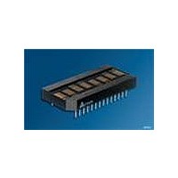
DISPLAY PROG 8CHAR .200" 5X7 HEG
Manufacturer
OSRAM Opto Semiconductors Inc
Series
Alphanumeric Programmable Display™r
Datasheet
1.PDSP2110.pdf
(14 pages)
Specifications of PDSP2114
Millicandela Rating
510µcd
Size / Dimension
1.70" L x 0.77" W x 0.21" H (42.67mm x 19.58mm x 5.31mm)
Color
Green
Configuration
5 x 7
Number Of Digits
8
Character Size
0.2 in
Illumination Color
High Efficiency Green
Wavelength
568 nm
Maximum Operating Temperature
+ 85 C
Minimum Operating Temperature
- 40 C
Luminous Intensity
510 ucd
Viewing Area (w X H)
2.85 mm x 4.81 mm
Display Type
5 x 7 Dot Matrix
Emitting Color
Hi-Eff. Green
Digit Size (in)
.2in
Viewing Area Height (mm)
4.81mm
Package Type
Panel
Operating Supply Voltage (min)
4.5V
Operating Supply Voltage (typ)
5V
Operating Supply Voltage (max)
5.5V
Operating Temperature Classification
Industrial
Operating Temp Range
-40C to 85C
Mounting
Through Hole
Pin Count
28
Total Thickness (mm)
5.1mm
Opto Display Type
Panel
Pattern Type
Dot Matrix
Lead Free Status / RoHS Status
Lead free / RoHS Compliant
Voltage - Forward (vf) Typ
-
Internal Connection
-
Lead Free Status / Rohs Status
Compliant
Other names
Q68000A8533


Top View
Pin Assignments
Pin
1
2
3
4
5
6
7
8
9
10
11
12
13
14
2006-01-23
28
1
0
Function
RST
FL
A0
A1
A2
A3
Substr. bias
No Connect
CLK I/O
WR
V
CLKSEL
1
CC
2
3
Digit
Pins
Pins
Pin
28
27
26
25
24
23
22
21
20
19
18
17
16
15
PDSP2110, PDSP2111, PDSP2112, PDSP2113, PDSP2114
4
5
Function
D7
D6
D5
D4
D3
D2
No Pin
D1
D0
No Connect
CE
GND (logic)
GND (supply)
6
IDPA5116
7
14
15
6
Pin Definitions
Pin
1
2
3
4
5
6
7-9
10
11
12
13
14
15
16
17
18
19
20
21
22
23
24
25
26
27
28
Function
RST
FL
A0
A1
A2
A3
Substr. bias Used to bias IC substrate, must be connected
No connect
CLKSEL
CLK I/O
WR
V
GND
GND
CE
No Connect —
D0
D1
No pin
D2
D3
D4
D5
D6
D7
CC
Definition
Used for initialization of a display and
sychronization of blinking for multiple displays
Low input accesses the Flash RAM
Address input LSB
Address input
Address input MSB
Mode selector
to V
display.
—
Selects internal/external clock source
Outputs master clock or inputs external clock
A low will write data into the display if CE is
low
Positive power supply input
Analog Ground for LED drivers
Digital Ground for internal logic
Enables access to the display
Data input LSB
Data input
—
Data input
Data input MSB, selects ROM, page 1 or 2
CC
. Can't be used to supply power to
Related parts for PDSP2114
Image
Part Number
Description
Manufacturer
Datasheet
Request
R

Part Number:
Description:
INTELLIGENT DISP 4CHAR 5X7 HERED
Manufacturer:
OSRAM Opto Semiconductors Inc
Datasheet:

Part Number:
Description:
DISPLAY 8DIGIT CERAMIC GREEN
Manufacturer:
OSRAM Opto Semiconductors Inc
Datasheet:

Part Number:
Description:
EMITTER IR 950NM 5MM SMD RADIAL
Manufacturer:
OSRAM Opto Semiconductors Inc
Datasheet:

Part Number:
Description:
LED TOPLED GREEN 570NM 2-PLCC
Manufacturer:
OSRAM Opto Semiconductors Inc
Datasheet:

Part Number:
Description:
INTERRUPTER RELFECT W/FILTR SMD
Manufacturer:
OSRAM Opto Semiconductors Inc
Datasheet:

Part Number:
Description:
LED Displays 5x7 Green 0.145 , 4-CHARACTER
Manufacturer:
OSRAM Opto Semiconductors Inc
Datasheet:

Part Number:
Description:
Q65110A4321_SIDELED PURE GREEN EOL150407
Manufacturer:
OSRAM Opto Semiconductors Inc
Datasheet:
Part Number:
Description:
Q65110A1202_RO DETECTOR 3/5MM_TR_RO
Manufacturer:
OSRAM Opto Semiconductors Inc
Datasheet:

Part Number:
Description:
PHOTODIODE 900NM 3MM W/FILTER
Manufacturer:
OSRAM Opto Semiconductors Inc
Datasheet:
Part Number:
Description:
INTELLIGENT DISP 4CHAR 5X7 HERED
Manufacturer:
OSRAM Opto Semiconductors Inc
Datasheet:
Part Number:
Description:
LED TOPLED GREEN 570NM 2-PLCC
Manufacturer:
OSRAM Opto Semiconductors Inc
Datasheet:
Part Number:
Description:
PHOTODIODE 900NM 3MM W/FILTER
Manufacturer:
OSRAM Opto Semiconductors Inc
Datasheet:

Part Number:
Description:
PHOTODIODE 850NM THRU-HOLE
Manufacturer:
OSRAM Opto Semiconductors Inc
Datasheet:

Part Number:
Description:
PHOTODIODE 880NM W/FILTER SMD
Manufacturer:
OSRAM Opto Semiconductors Inc
Datasheet: