PDSP1883 OSRAM Opto Semiconductors Inc, PDSP1883 Datasheet
PDSP1883
Specifications of PDSP1883


Related parts for PDSP1883


PDSP1883 Summary of contents
Page 1
... Green High Efficiency Green PDSP1884 DESCRIPTION The PDSP1880 (Red), PDSP1881 (Yellow), PDSP1882 (High Efficiency Red), PDSP1883 (Green), and PDSP1884 (High Efficiency Green) are eight digit dot matrix, alphanumeric Programmable Displays. The 4.70 mm (0.180’’) high digits are packaged in a rug- ged, high quality, optically transparent, 7.62 mm (0.300’ ...
Page 2
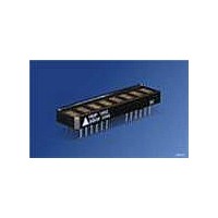
... PDSP1880, PDSP1881, PDSP1882, PDSP1883, PDSP1884 Ordering Information Type Color of Emission PDSP1880 red PDSP1881 yellow PDSP1882 high efficiency red PDSP1883 green PDSP1884 high efficiency green Package Outlines Pin 1 Identifier Date Code PDSP188X Z OSRAM 5.08 (0.200) Pin 1 Indicator 2.54 (0.100 Pin 1 Identifier 2006-03-30 ...
Page 3
... PDSP1880, PDSP1881, PDSP1882, PDSP1883, PDSP1884 Maximum Ratings (T =25°C) A Parameter Operating temperature range Storage temperature range V DC Supply Voltage, to GND CC (max. voltage with no LEDs on) V Operating Voltage, to GND CC (max. voltage with 20 dots/digits on) Input Voltage Levels, all inputs Solder Temperature 1.59 mm (0.063“) below seating plane, t < 5.0 s Relative Humidity (non-condensing) ESD (100 pF, 1.5 kΩ ...
Page 4
... PDSP1880, PDSP1881, PDSP1882, PDSP1883, PDSP1884 Enlarged Character Format 2.49 (0.098 0.56 (0.022) typ. Write Cycle Timing Diagram A0- acs CE WR D0-D7 2006-03-30 Dimensions in mm (inch) Switching Specifications (over operating temperature range and V Symbol T acc T acc acs ach R4 T cer R5 T ces R6 T ces ...
Page 5
... PDSP1880, PDSP1881, PDSP1882, PDSP1883, PDSP1884 Read Cycle Timing Diagram A0- acs CE RD D0-D7 Character Set D0 D1 ASCII CODE HEX Notes: 1. Upon power up, the device will initialize in a random state. 2. X=don’t care. 2006-03-30 T acc ces UDC UDC UDC UDC UDC UDC UDC ...
Page 6
... PDSP1880, PDSP1881, PDSP1882, PDSP1883, PDSP1884 DC Electrical Characteristics at 25°C Parameters Blank dots/digit dots/digit (with pull-up) ILP Input Leakage I (no pull-up) IL Input Leakage Input Voltage High Input Voltage Low IL V (D0–D7), Output Voltage Low OL (CLK), Output Voltage Low Output Voltage High OH θ ...
Page 7
... PDSP1880, PDSP1881, PDSP1882, PDSP1883, PDSP1884 Top View Pin Assignments Pin # Name Symbol Definition 1 Reset RST Initializes display; clears Character RAM (20H), Flash RAM (00H), control word (00H), and resets internal counters. UDC Address Register and UDC RAM unaffected. 2 Flash FL Accesses Flash RAM. Address inputs A0– ...
Page 8
... PDSP1880, PDSP1881, PDSP1882, PDSP1883, PDSP1884 Cascading Diagram RST Display D0-D7 A0-A4 Data I/O Address Address Decoder Block Diagram Character Character 4 Data Bus 2006-03- RST CLK CLK I/O SEL more displays in between CE Address Decode Chip OSC 32 7 Counter Counter 3 Counter Row Drivers ...
Page 9
... PDSP1880, PDSP1881, PDSP1882, PDSP1883, PDSP1884 Functional Description The display's user interface is organized into five memory areas. They are accessed using the Flash Input and address lines, A3 and A4. All the listed RAMs and Registers may be read or writ- ten through the data bus. See Table „Memory Selection“ (page 9). ...
Page 10
... PDSP1880, PDSP1881, PDSP1882, PDSP1883, PDSP1884 The display Blink works the same way as the Flash Enable but causes all twenty column drivers to cycle at 2.0 Hz thereby making all eight digits blink at 2.0 Hz. The Self Test function of the IC consists of two internal routines which exercise major portions of the IC and illuminates all the LEDs ...
Page 11
... PDSP1880, PDSP1881, PDSP1882, PDSP1883, PDSP1884 Flash RAM The Flash RAM allows the display to flash one or more of the char- acters being displayed. The Flash Ram is accessed by setting FL low. A4 and A3 are ignored. The Flash RAM bit RAM with each bit corresponding to a digit address. Digit the left side of the display and digit the right side of the display. Address lines, A2– ...
Page 12
... PDSP1880, PDSP1881, PDSP1882, PDSP1883, PDSP1884 The second routine provides a visual test of the LEDs. This is accomplished by writing checkered and inversed checkered pat- terns to the display. Each pattern is displayed for approximately 2.0 sec. During the self test function the display must not be accessed. The time needed to execute the self test function is cal- culated by multiplying the clock time by 262,144 (typical time ≈ ...
Page 13
... PDSP1880, PDSP1881, PDSP1882, PDSP1883, PDSP1884 Display Cycle Using Built-in ROM Example Display message “Showtime.” Digit 0 is leftmost—closest to pin 1. Logic levels: 0=Low, 1=High, X=Don’t care. RST Displaying User Defined Character Example Load character “A” into UDC-5 and then display it in digit 2. ...
Page 14
... The PDSP1883 should be matched with a yellow-green band-pass fil- ter that peaks at 565 nm. For displays of multiple colors, neutral density grey filters offer the best compromise. ...
Page 15
... PDSP1880, PDSP1881, PDSP1882, PDSP1883, PDSP1884 Revision History: 2006-03-30 Previous Version: 2004-12-09 Page Subjects (major changes since last revision) all Lead free device ublished by P OSRAM Opto Semiconductors GmbH Wernerwerkstrasse 2, D-93049 Regensburg www.osram-os.com © All Rights Reserved. Attention please! The information describes the type of component and shall not be considered as assured characteristics. ...