IPD2133 OSRAM Opto Semiconductors Inc, IPD2133 Datasheet - Page 10
IPD2133
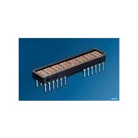
Manufacturer Part Number
IPD2133
Description
DISPLAY 8DIGIT CERAMIC GREEN
Manufacturer
OSRAM Opto Semiconductors Inc
Series
Alphanumeric Programmable Display™r
Datasheet
1.IPD2131.pdf
(16 pages)
Specifications of IPD2133
Millicandela Rating
500µcd
Size / Dimension
1.68" L x 0.39" W x 0.21" H (42.7mm x 4.8mm x 5.3mm)
Color
Green
Configuration
5 x 7
Number Of Digits
8
Character Size
0.2 in
Illumination Color
High Efficiency Green
Wavelength
568 nm
Maximum Operating Temperature
+ 100 C
Minimum Operating Temperature
- 55 C
Luminous Intensity
500 ucd
Viewing Area (w X H)
2.8 mm x 4.8 mm
Display Type
5 x 7 Dot Matrix
Emitting Color
Hi-Eff. Green
Digit Size (in)
.2in
Viewing Area Height (mm)
4.8mm
Viewing Area Length (mm)
2.8mm
Package Type
Panel
Operating Supply Voltage (min)
4.5V
Operating Supply Voltage (typ)
5V
Operating Supply Voltage (max)
5.5V
Operating Temperature Classification
Industrial
Operating Temp Range
-55C to 100C
Mounting
Through Hole
Pin Count
24
Total Thickness (mm)
4.6mm
Opto Display Type
Panel
Pattern Type
Dot Matrix
Lead Free Status / RoHS Status
Lead free / RoHS Compliant
Voltage - Forward (vf) Typ
-
Internal Connection
-
Lead Free Status / Rohs Status
Compliant
Other names
Q68000A8906
Available stocks
Company
Part Number
Manufacturer
Quantity
Price


Memory Selection
FL
0
1
1
1
1
Theory of Operation
The IPD213X Display is designed to work with all major micropro-
cessors. Data entry is via an eight bit parallel bus. Three bits of
address route the data to the proper digit location in the RAM.
Standard control signals like WR and CE allow the data to be writ-
ten into the display.
D0–D7 data bits are used for both Character RAM and control
word data input. A3 acts as the mode selector.
If A3=1, character RAM is selected. Then input data bit D7 will
determine whether input data bits D0–D6 is ASCII coded data
(D7=0) or UDC data (D7=1). See section on „UDC Address Regis-
ter and UDC RAM“ (page 11).
For normal operation FL pin should be held high. When FL is held
low, Flash RAM is accessed to set character blinking.
The seven bit ASCII code is decoded by the Character ROM to
generate Column data. Twenty columns worth of data is sent out
each display cycle, and it takes fourteen display cycles to write into
eight digits.
The rows are multiplexed in two sets of seven rows each. The
internal timing and control logic synchronizes the turning on of
rows and presentation of column data to assure proper display
operation.
Power Up Sequence
Upon power up the display will come on at random. Thus the dis-
play should be reset on power-up. Reset will clear the Flash
RAM, Control Word Register and reset the internal counter. All
the digits will show blanks and display brightness level will be
100%.
The display must not be accessed until three clock pulses (110 µs
minimum using the internal clock) after the rising edge of the reset
line.
2006-04-04
1
A4
X
0
0
1
A3
X
0
1
1
0
Section of Memory
Flash RAM
UDC Address Register
UDC RAM
Character RAM
Control Word Register
10
A2–A0
Character Address
Don’t Care
Row Address
Character Address
Don’t Care
Microprocessor Interface
The interface to a microprocessor is through the 8-bit data bus
(D0–D7), the 4-bit address bus (A0–A3) and control lines FL , CE
and WR.
To write data (ASCII/Control Word) into the display CE should be
held low, address and data signals stable and WR should be
brought low. The data is written on the low to high transition of
WR.
The Control Word is decoded by the Control Word Decode Logic.
Each code has a different function. The code for display brightness
changes the duty cycle for the column drivers. The peak LED cur-
rent stays the same but the average LED current diminishes
depending on the intensity level.
The character Flash Enable causes 2.0 Hz coming out of the
counter to be ANDED with the column drive signal to make the col-
umn driver cycle at 2.0 Hz. Thus the character flashes at 2.0 Hz.
The display Blink works the same way as the Flash Enable but
causes all twenty column drivers to cycle at 2.0 Hz thereby making
all eight digits blink at 2.0 Hz.
The Self Test function of the IC consists of two internal routines
which exercise major portions of the IC and illuminates all the
LEDs.
Clear bit clears the character RAM and writes a blank into the dis-
play memory. It however does not clear the control word.
ASCII Data or Control Word Data can be written into the display
at this point. For multiple display operation, CLK I/O must be
properly selected. CLK I/O will output the internal clock if CLK-
SEL=1, or will allow input from an external clock if CLKSEL=0.
IPD2131, IPD2132, IPD2133
Data Bits Used
D0
D3–D0
D4–D0
D7–D0
D7–D0
Related parts for IPD2133
Image
Part Number
Description
Manufacturer
Datasheet
Request
R

Part Number:
Description:
INTELLIGENT DISP 4CHAR 5X7 HERED
Manufacturer:
OSRAM Opto Semiconductors Inc
Datasheet:

Part Number:
Description:
EMITTER IR 950NM 5MM SMD RADIAL
Manufacturer:
OSRAM Opto Semiconductors Inc
Datasheet:

Part Number:
Description:
LED TOPLED GREEN 570NM 2-PLCC
Manufacturer:
OSRAM Opto Semiconductors Inc
Datasheet:

Part Number:
Description:
INTERRUPTER RELFECT W/FILTR SMD
Manufacturer:
OSRAM Opto Semiconductors Inc
Datasheet:

Part Number:
Description:
LED Displays 5x7 Green 0.145 , 4-CHARACTER
Manufacturer:
OSRAM Opto Semiconductors Inc
Datasheet:

Part Number:
Description:
Q65110A4321_SIDELED PURE GREEN EOL150407
Manufacturer:
OSRAM Opto Semiconductors Inc
Datasheet:
Part Number:
Description:
Q65110A1202_RO DETECTOR 3/5MM_TR_RO
Manufacturer:
OSRAM Opto Semiconductors Inc
Datasheet:

Part Number:
Description:
PHOTODIODE 900NM 3MM W/FILTER
Manufacturer:
OSRAM Opto Semiconductors Inc
Datasheet:

Part Number:
Description:
PHOTODIODE 860NM 3MM CLEAR
Manufacturer:
OSRAM Opto Semiconductors Inc
Datasheet:
Part Number:
Description:
INTELLIGENT DISP 4CHAR 5X7 HERED
Manufacturer:
OSRAM Opto Semiconductors Inc
Datasheet:
Part Number:
Description:
LED TOPLED GREEN 570NM 2-PLCC
Manufacturer:
OSRAM Opto Semiconductors Inc
Datasheet:
Part Number:
Description:
PHOTODIODE 900NM 3MM W/FILTER
Manufacturer:
OSRAM Opto Semiconductors Inc
Datasheet:

Part Number:
Description:
PHOTODIODE 850NM THRU-HOLE
Manufacturer:
OSRAM Opto Semiconductors Inc
Datasheet:

Part Number:
Description:
PHOTODIODE 880NM W/FILTER SMD
Manufacturer:
OSRAM Opto Semiconductors Inc
Datasheet: