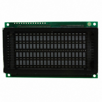
M0420SD-204SDAR1-3 Newhaven Display, M0420SD-204SDAR1-3 Datasheet - Page 13

M0420SD-204SDAR1-3
Manufacturer Part Number
M0420SD-204SDAR1-3
Description
MODULE VF CHAR 4X20 4.84MM
Manufacturer
Newhaven Display
Datasheet
1.M0420SD-204SDAR1-3.pdf
(24 pages)
Specifications of M0420SD-204SDAR1-3
Outline L X W X H
100.00mm x 60.00mm x 20.60mm
Viewing Area
73.60mm L x 30.96mm W
Display Format
20 x 4
Display Type
Character
Format
5 x 8 Dots
Voltage - Supply
5V
Character Size
4.84mm H x 2.35mm W
Operating Temperature
-40°C ~ 85°C
Product
Character Display Modules
Character Count X Line
20 x 4
Module Size (w X H X T)
100 mm x 60 mm x 20.6 mm
Voltage Rating
5 V
Operating Temperature Range
- 40 C to + 85 C
Dot Format
5 x 8
Viewing Area (w X H)
73.6 mm x 30.96 mm
Lead Free Status / RoHS Status
Lead free / RoHS Compliant
Interface
-
Number Of Dots
-
Lead Free Status / Rohs Status
Lead free / RoHS Compliant
STANDARD NAME:
5.1.2 INTEL I80-TYPE MODE
This mode uses the Read (RD/) and Write (WR/) control signals to transfer information.
Instructions/data are written to the module on the rising edge of WR/ and are read from the
modules after the falling edge of RD/.
5.2 SYNCHRONOUS SERIAL INTERFACE MODE
In the synchronous serial interface mode, instructions and data are sent between the host and the
module using 8-bit bytes. Two bytes are required per read/write cycle and are transmitted MSB
first. The start byte contains 5 high bits, the Read/Write (R/W) control bit, the Register Select
(RS) control bit, and a low bit. The following byte contains the instruction/data bits. The R/W
bit determines whether the cycle is a read (high) or a write (low) cycle. The RS bit is used to
identify the second byte as an instruction (low) or data (high).
This mode uses the Strobe (STB) control signal, Serial Clock (SCK) input, and Serial I/O
(SI/SO) line to transfer information. In a write cycle, bits are clocked into the modules on the
rising edge of SCK. In a read cycle, bits in the start byte are clocked into the modules on the
rising edge of SCK. After the minimum wait time, each bit in the instruction/data byte can be
read from the modules after each falling edge of SCK. Each read/write cycle begins on the
falling edge of STB and ends on the rising edge. To be a valid read/write cycle, the STB must go
high at the end of the cycle.
DB7
WR/
DB6
DB0
RD/
RS
Figure 10. Typical 8-Bit Parallel Interface Sequence Using I80-Type Mode
Write instruction
IB7
IB6
IB0
Write instruction
IB7
IB6
IB0
M0420SD-204SDAR1-3
DOCUMENT NUMBER:
DATE PRINTED:
Read instruction
BF= '0'
IB6
IB0
SHEET:
REV:
Write data
DB7
DB6
DB0
13 of 24
00


