LE A S2W-MXMZ-34 OSRAM Opto Semiconductors Inc, LE A S2W-MXMZ-34 Datasheet
LE A S2W-MXMZ-34
Specifications of LE A S2W-MXMZ-34
Q65110A8181


Related parts for LE A S2W-MXMZ-34


LE A S2W-MXMZ-34 Summary of contents
Page 1
... Digitalkameras, MP3-Player, Spielkonsolen) • Accessory - Projektion • Stimmungslicht • Gebäudebeleuchtung (Effekt- und Akzentbeleuchtung) 2009-03- S2W Features • package: compact lightsource in multi chip SMT technology with glass window on top • feature of the device: outstanding brightness and luminance due to pure surface emission and low R • ...
Page 2
... LE B S2W-KYLY-23 blue Bestellinformation Ordering Information Typ Type LE A S2W-MXMZ- S2W-NYPY- S2W-KYLY-23 Anm.: Die oben genannten Typbezeichnungen umfassen die bestellbaren Selektionen. Diese bestehen aus wenigen Helligkeitsgruppen (siehe Seite 6 für nähere Informationen). Es wird nur eine einzige Helligkeitsgruppe pro Gurt geliefert. Z.B bedeutet, dass auf dem Gurt nur eine der Helligkeitsgruppen -MX, -MY oder -MZ enthalten ist. Um die Liefersicherheit zu gewä ...
Page 3
... Forward current per chip =25°C) S Stoßstrom pro Chip DC Surge current per chip DC t ≤ μ 0.1; =25°C A Sperrspannung pro Chip DC Reverse voltage per chip =25°C) S 2009-03- S2W S2W S2W Symbol Symbol amber stg (min.) F (max not designed for reverse R 3 Werte ...
Page 4
... Seite 20 (min (typ (max.) F (max η (typ.) opt (typ.) A Color (typ Φ (typ.) V 120 S2W S2W S2W Werte Values amber true blue green 617 525 465 613 521 458 617 529 464 625 537 470 120 2.1 2.9 2.5 3.6 3.3 4 ...
Page 5
... Seite 20 3) page 20 amber true green max. min. 619 521 625 527 533 Wellenlänge Wavelength S2W S2W S2W 1) Seite 20 Lichtstärke Luminous Intensity Ι (cd (typ.) 75 (typ.) 87 (typ.) 120 (typ.) 140 (typ.) 160 (typ.) 190 (typ.) 30 (typ.) 35 (typ.) 40 (typ.) 47 (typ ...
Page 6
... Relative Spectral Emission per Chip λ spektrale Augenempfindlichkeit / Standard eye response curve Φ λ ° 700 mA rel A F 100 % Φ rel 400 450 2009-03- S2W S2W S2W 2) Seite 20 2) page 20 V blue λ amber true green 500 550 6 OHL04115 600 650 nm 700 λ ...
Page 7
... Relativer zonaler Lichtstromanteil 2) page 20 Relative Partial flux ϕ Φ Φ (90° ° 2009-03-17 30˚ 20˚ 10˚ 0.8 0.6 0.4 2) Seite S2W S2W S2W 0˚ 1.0 0.8 0.6 0.4 0.2 0 0˚ 20˚ 40˚ 60˚ 80˚ OHL03736 100˚ 120˚ ...
Page 8
... V Φ (700 mA 2009-03-17 Durchlassstrom pro Chip Forward Current per chip OHL02681 V 3 Relativer Lichtstrom Relative Luminous Flux Φ /Φ V OHL12619 S2W S2W S2W 2) Seite 20 2) page ° S2W S2W 2.0 2.5 3.0 3 Seite page S2W S2W (700 mA ° Φ V Φ V (700 mA) ...
Page 9
... Seite 20 Dominante Wellenlänge 2) page 20 Dominant Wavelength Δλ ° S2W dom F A 2009-03- S2W S2W S2W Dominante Wellenlänge 2) page 20 Dominant Wavelength λ ° S2W dom Seite 20 ...
Page 10
... I = 700 mA Relative Vorwärtsspannung pro Chip Relative Forward Voltage per chip ΔV (25 ° 700 mA 2009-03- S2W S2W S2W 2) Seite 20 2) page S2W 2) Seite 20 Relative Vorwärtsspannung pro Chip 2) page 20 Relative Forward Voltage per chip Δ S2W = page S2W (25 ° 700 mA ...
Page 11
... Seite 20 Relative Lichtstrom 2) page 20 Relative Luminous Flux Φ /Φ (25 ° 700 mA Seite 20 Relative Lichtstrom 2) page 20 Relative Luminous Flux Φ /Φ (25 ° 700 mA 2009-03- S2W Relative Lichtstrom Relative Luminous Flux Φ /Φ S2W S2W S2W S2W 2) Seite 20 2) page S2W (25 ° 700 mA ...
Page 12
... Seite 20 Dominante Wellenlänge 2) page 20 Dominant Wavelength Δλ 700 mA S2W dom Seite 20 Dominante Wellenlänge 2) page 20 Dominant Wavelength Δλ 700 mA S2W dom j F 2009-03- S2W S2W S2W Dominante Wellenlänge 2) page 20 Dominant Wavelength Δλ 700 mA S2W dom Seite 20 ...
Page 13
... F Maximal zulässiger Durchlassstrom Max. Permissible Forward Current for true green / blue 1 chip operated F 2009-03- S2W S2W S2W Maximal zulässiger Durchlassstrom Max. Permissible Forward Current for amber 4 chips operated F Maximal zulässiger Durchlassstrom Max. Permissible Forward Current ...
Page 14
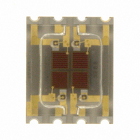
... LE A S2W 1-4: amber LE T S2W 1-4: true green LE B S2W 1-4: blue Gewicht / Approx. weight: 2009-03- S2W S2W S2W Pin-Assignment: P1: Cathode; Chip 1 P2: Anode; Chip 1 P3: Cathode; Chip 2 P4: Anode; Chip 2 P5: Cathode; Chip 3 P6: Anode; Chip 3 P7: Cathode; Chip 4 P8: Anode ...
Page 15
... Seite 20 Verpackung 6) page 20 Method of Packing Elektrisches Ersatzschaltbild Equivalent Circuit Diagram 2009-03- S2W S2W S2W 500 St. pro Rolle = Verpackungseinheit 500 pcs. per reel = packing unit 15 ...
Page 16
... Ramp K/s (max) 25 ˚ 2009-03- S2W S2W S2W ® Reflow Löten ® Reflow Soldering Vorbehandlung nach JEDEC Level 2 Preconditioning acc. to JEDEC Level 2 Maximum Solder Profile Recommended Solder Profile Minimum Solder Profile 120 s max 100 150 ...
Page 17
... ± 0.1 2 ± 0.05 (0.315 ± 0.004) (0.079 ± 0.002 min 1 12 (0.488 + 0.079) 60 (2.362 S2W S2W S2W Bin1: Bin Information Color 1 Lx xxxx Bin2: Product Name Bin3: ML Temp ST RoHS Compliant 2 260 C RT Additional TEXT R077 DEMY PACKVAR: Packing Type (G) GROUP: ...
Page 18
... If dry. adequately desiccant change still parts 5% wet, If MIL-I-8835 Indicator Humidity Desiccant Barcode label Länge / length 200 ±5 (7,874 ±0,1968 S2W S2W S2W Humidity indicator Barcode label OHA00539 Barcode label Packing Sealing label Höhe / height 30 ±5 (1,1811 ±0,1968) OHA02044 ...
Page 19
... Components used in life-support devices or systems must be expressly authorized for such purpose! Critical 10) page 20 components may only be used in life-support devices or systems OS. 2009-03- S2W S2W S2W 11) page 20 with the express written approval of OSRAM 19 Date of change 2008-11-13 2009-03-03 ...
Page 20
... Systemen oder Systems S2W S2W S2W Brightness groups are tested at a current pulse duration and a tolerance of ± 11%. Due to the special conditions of the manufacturing processes of LED, the typical data or calculated correlations of technical parameters can only reflect statistical figures. These do not necessarily correspond ...