LE UW S2W-NZPZ-FRKV OSRAM Opto Semiconductors Inc, LE UW S2W-NZPZ-FRKV Datasheet
LE UW S2W-NZPZ-FRKV
Specifications of LE UW S2W-NZPZ-FRKV


Related parts for LE UW S2W-NZPZ-FRKV


LE UW S2W-NZPZ-FRKV Summary of contents
Page 1
... OSTAR - SMT Lead (Pb) Free Product - RoHS Compliant LE UW S2W Vorläufige Daten / preliminary data Besondere Merkmale • Gehäusetyp: Kompakte Lichtquelle in Multi-Chip SMT Technologie mit Glasabdeckung • Besonderheit des Bauteils: extrem hohe Helligkeit und Leuchtdichte dank Oberflächenemission und niedrigem R • Farbort 0,31 0,32 nach CIE 1931 (weiß ...
Page 2
... The above Type Numbers represent the order groups which include only a few brightness groups (see page 7 for explanation). Only one group will be shipped on each reel (there will be no mixing of two groups on each reel). E. S2W-NZPZ-FRKV means that only one group NZ, PX will be shippable for any one reel. ...
Page 3
... S Stoßstrom Surge current ≤ μ 0. °C A Sperrspannung Reverse voltage T ( =25°C) A 2009-03-17 Symbol Symbol stg T j (min (max not designed for R reverse operation S2W Werte Einheit Values Unit – 40 … °C – 40 … °C 125 °C 100 mA 1000 mA 2000 mA V ...
Page 4
... Seite (min.) F (typ (max (max.) R η (typ.) opt η (typ.) opt (typ.) A Chip (typ S2W Werte Values 0.31 0.32 120 2.9 3.6 4.2 not designed for reverse operation 21*10 3.1 (typ.) Einheit Unit – – Grad deg μ A lm/W lm/W mm² ...
Page 5
... Cx Cy 0.388 0.378 0.370 0.380 0.362 0.370 0.377 0.369 0.349 0.362 0.369 0.356 0.337 0.349 0.356 0.343 0.39 0.38 5700 K 0.37 0.36 6500 K 0. 0.33 8000 0.29 0.28 0. S2W 5000 ...
Page 6
... Gruppe Group HV 0.330 HU 0.337 0.346 0.339 0.321 HT 0.330 0.339 0.329 0.311 HS 0.321 0.329 0.319 0.305 HR 0.311 0.319 0.312 S2W Cx Cy 0.329 0.362 0.329 0.369 0.338 0.378 0.338 0.370 0.329 0.354 0.329 0.362 0.338 0.370 0.338 0.362 0.329 0.342 0.329 0.354 0.338 ...
Page 7
... No packing unit ever contains more than one group for each selection. 2009-03-17 Cy 0.307 0.313 0.330 0.321 0.297 0.307 0.321 0.311 0.289 0.297 0.311 0.302 Lichtstrom Luminous Flux Φ (lm) V 390 ... 450 ... 520 ... 610 ... Wellenlänge Wavelength S2W 2) Seite 19 2) page 19 450 520 610 710 ...
Page 8
... Relative spektrale Emission Relative Spectral Emission λ spektrale Augenempfindlichkeit / Standard eye response curve Φ λ °C, rel board F 100 % Φ rel 400 450 2009-03-17 2) Seite 19 2) page 19 = 700 mA 500 550 8 V λ 600 650 700 LE UW S2W OHL13926 nm 750 λ ...
Page 9
... Relativer zonaler Lichtstromanteil 2) page 19 Relative Partial flux ϕ Φ Φ (90° ° 2009-03-17 30˚ 20˚ 10˚ 0˚ 1.0 0.8 0.6 0.4 0.2 0 0.6 0.4 0˚ 2) Seite 19 9 20˚ 40˚ 60˚ 80˚ 100˚ S2W OHL03736 120˚ ...
Page 10
... Seite 19 Durchlassstrom pro Chip 2) page 19 Forward Current per chip = ° board 2) Seite 19 Farbortverschiebung Chromaticity Coordinate Shift ΔCx, Δ °C F board 2009-03-17 Relative Lichtstrom Relative Luminous Flux Φ /Φ (700 mA page S2W 2) 5) Seite page °C F board ...
Page 11
... Relative Vorwärtsspannung pro Chip Relative Forward Voltage per chip ΔV (25 ° 700 Seite 19 Farbortverschiebung Chromaticity Coordinate Shift ΔCx, Δ 700 2009-03-17 2) Seite 19 Relative Lichtstrom 2) page 19 Relative Luminous Flux Φ /Φ (25 ° page S2W 2) Seite 19 2) page 700 ...
Page 12
... Maximal zulässiger Durchlassstrom Max. Permissible Forward Current for 4 chips operated F S 2009-03-17 Maximal zulässiger Durchlassstrom Max. Permissible Forward Current for 1 chip operated S2W ...
Page 13
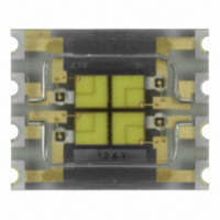
... Seite 19 Maßzeichnung 6) page 19 Package Outlines Chip-Position: 1-4: ultra white Kathodenkennung: Cathode mark: Gewicht / Approx. weight: 2009-03-17 Pin-Assignment: P1: Cathode; Chip 1 P2: Anode; Chip 1 P3: Cathode; Chip 2 P4: Anode; Chip 2 P5: Cathode; Chip 3 P6: Anode; Chip 3 P7: Cathode; Chip 4 P8: Anode; Chip S2W ...
Page 14
... Verpackung / Polarität und Lage Method of Packing / Polarity and Orientation Elektrisches Ersatzschaltbild Equivalent Circuit Diagram 2009-03-17 6) Seite 19 6) page S2W ...
Page 15
... Vorbehandlung nach JEDEC Level 2 Preconditioning acc. to JEDEC Level 2 (nach J-STD-020B) (acc. to J-STD-020B) Maximum Solder Profile Recommended Solder Profile Minimum Solder Profile 120 s max 100 150 S2W 6) Seite 19 6) page 19 OHLA0687 +0 ˚C 260 ˚C -5 ˚C 245 ˚C ±5 ˚C +5 ˚C 235 ˚C -0 ˚ ...
Page 16
... GROUP Forward Voltage Group Wavelength Group Brightness Group OHA12043 Label Direction of unreeling Gurtvorlauf: 400 mm Leader: 400 mm Gurtende: 160 mm Trailer: 160 1.5 + 0.1 1.75 ± 0.1 (0.059 + 0.004) (0.069 ± 0.004 S2W OHAY0324 F 5.5 ± 0.05 (0.217 ± 0.002 max 18.4 (0.724) ...
Page 17
... If desiccant change dry. adequately still parts 5% wet, If MIL-I-8835 Indicator Humidity Desiccant . Barcode label Länge / length 200 ±5 (7,874 ±0,1968 S2W Humidity indicator Barcode label OHA00539 Barcode label Packing Sealing label Höhe / height 30 ±5 (1,1811 ±0,1968) OHA02044 ...
Page 18
... Components used in life-support devices or systems must be expressly authorized for such purpose! Critical 7) page 19 components may only be used in life-support devices or systems OSRAM OS. 2009-03-17 8) page 19 with the express written approval S2W Date of change 2008-11-13 2009-03-17 ...
Page 19
... Life support devices or systems are intended ( implanted in the human body, or (b) to support and/or maintain and sustain human life. If they fail reasonable to assume that the health and the life of the user may be endangered S2W figures. These do not necessarily ...