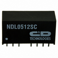
NDL0512SC Murata Power Solutions Inc, NDL0512SC Datasheet - Page 3

NDL0512SC
Manufacturer Part Number
NDL0512SC
Description
CONV DC/DC 2W 5VIN 12VOUT SIP
Manufacturer
Murata Power Solutions Inc
Series
NDLr
Type
Isolatedr
Datasheet
1.NDL2405SC.pdf
(4 pages)
Specifications of NDL0512SC
Output
12V
Number Of Outputs
1
Power (watts)
2W
Mounting Type
Through Hole
Voltage - Input
4.5 ~ 9V
Package / Case
8-SIP Module (7 Leads)
1st Output
12 VDC @ 167mA
Size / Dimension
0.86" L x 0.36" W x 0.44" H (21.8mm x 9.1mm x 11.2mm)
Power (watts) - Rated
2W
Operating Temperature
-40°C ~ 85°C
Efficiency
71%
Approvals
UL
Dc / Dc Converter O/p Type
Fixed
No. Of Outputs
1
Input Voltage
4.5V To 9V
Power Rating
2W
Output Voltage
12V
Output Current
167mA
Supply Voltage
5V
Dc / Dc Converter Case Style
SIP
Product
Isolated
Output Power
2 W
Input Voltage Range
4.5 V to 9 V
Input Voltage (nominal)
5 V
Output Voltage (channel 1)
12 V
Output Current (channel 1)
167 mA
Isolation Voltage
1 KV
Package / Case Size
SIP
Lead Free Status / RoHS Status
Lead free / RoHS Compliant
3rd Output
-
2nd Output
-
4th Output
-
Lead Free Status / Rohs Status
Lead free / RoHS Compliant
Other names
811-1357-5
Available stocks
Company
Part Number
Manufacturer
Quantity
Price
APPLICATION NOTES
External capacitance
Control Pin
Pin 8 (C
Minimum load
RoHS COMPLIANT INFORMATION
www.murata-ps.com
Although these converters will work without external capacitors, they are necessary
in order to guarantee the full parametric performance over the full line and load
range. All parts have been tested and characterized using the following values and
test circuit.
The NDL converters have a shutdown feature which enables the user to put the converter into a low power state. The control pin connects directly to the base of an internal
transistor, and the switch off mechanism for the NDL works by forward biasing this NPN transistor. If the pin is left open (high impedance), the converter will be ON (there is
no allowed low state for this pin), but once a control voltage is applied with suffi cient drive current, the converter will be switched OFF. A suitable application circuit is shown
below.
This pin provides a connection point to the main reservoir capacitor. Additional capacitance can be added from this pin to pin 7. Any lower ESR capacitor will remove ripple
and noise to some degree. The benefi t of this access point over simple additional output capacitance is that it precedes the output fi lter inductor. Maximum values of external
capacitance will be dependent on the output voltage, the loading of the converter and the desired ripple fi gure. Values can be up to 100μF.
The minimum load for correct operation is 25% of the full rated load across the specifi ed input voltage range. Lower loads may cause a signifi cant increase in output ripple
The minimum load for correct operation is 25% of the full rated load across the specifi ed input voltage range. Lower loads may cause a signifi cant increase in output ripple
and may cause the output voltage to exceed its specifi cation transiently during power-down when the input voltage also falls below its rated minimum.
and may cause the output voltage to exceed its specifi cation transiently during power-down when the input voltage also falls below its rated minimum.
Test circuit
For further information, please visit www.murata-ps.com/rohs
S
)
OV
V
C
-V
V
IN
IN
R
Supply + V
Supply - V
1
This series is compatible with RoHS soldering
systems with a peak wave solder temperature of
300ºC for 10 seconds. The pin termination fi nish
on this product series is Tin Plate, Hot Dipped
over Matte Tin with Nickel Preplate. The series
is backward compatible with Sn/Pb soldering
systems.
D
1
IN
IN
CTRL
C
IN
NDL
Q
1
R
2
+ V
- V
IN
IN
NDL
NDL05 POWER DERATING CURVE
+ V
Isolated 2W Wide Input Single Output DC/DC Converters
- V
D
low. From the NDL specifi cation, the drive current to operate this function
is recommended to be 10mA, and hence the value of R
follows:
R
Assuming V
R
OUT
OUT
1
1
1
=
=
(e.g. 1N4001) is required to provide high impedence when the signal is
Input Voltage (V)
Technical enquiries email: mk@murata-ps.com, tel: +44 (0)1908 615232
5 - 0.7 - 1.0
V
10 x 10
C
24 & 48
- V
5 & 12
I
C
D
1.75
C
=5V, V
2.5
2.0
1.5
1.0
0.5
- V
-3
0
Q
4.5
= 330Ω
D
=0.7V and V
5
Isolation voltage (V)
C
OUT
6
Q
=1V:
100μF, 25V
10μF, 200V
Value
C
IN
2009/10/29 KDC_NDLC.F03 Page 3 of 4
7
8
NDL Series
1
can be derived as
9
100μF, 25V
100μF, 25V
C
OUT


