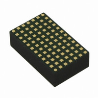
LTM4618EV#PBF Linear Technology, LTM4618EV#PBF Datasheet - Page 4

LTM4618EV#PBF
Manufacturer Part Number
LTM4618EV#PBF
Description
IC DC-DC UMODULE BUCK 6A 84-LGA
Manufacturer
Linear Technology
Series
µModuler
Type
Point of Load (POL) Non-Isolatedr
Datasheet
1.LTM4618EVPBF.pdf
(24 pages)
Specifications of LTM4618EV#PBF
Output
0.8 ~ 5 V
Number Of Outputs
1
Power (watts)
30W
Mounting Type
Surface Mount
Voltage - Input
4.5 ~ 26.5 V
Package / Case
84-LGA
1st Output
0.8 ~ 5 VDC @ 6A
Size / Dimension
0.59" L x 0.35" W x 0.17" H (15mm x 9mm x 4.32mm)
Power (watts) - Rated
30W
Operating Temperature
-40°C ~ 125°C
Lead Free Status / RoHS Status
Lead free / RoHS Compliant
3rd Output
-
2nd Output
-
Available stocks
Company
Part Number
Manufacturer
Quantity
Price
ELECTRICAL CHARACTERISTICS
LTM4618
operating temperature range, otherwise specifi cations are at T
Note 1: Stresses beyond those listed under Absolute Maximum Ratings
may cause permanent damage to the device. Exposure to any Absolute
Maximum Rating condition for extended periods may affect device
reliability and lifetime.
Note 2: The LTM4618 is tested under pulsed load conditions such that
T
over the 0°C to 125°C internal operating temperature range. Specifi cations
over the full –40°C to 125°C internal operating temperature range are
assured by design, characterization and correlation with statistical process
controls. The LTM4618I is guaranteed to meet specifi cations over the full
SYMBOL
f
V
V
R
I
V
V
R
PGOOD Output
V
I
V
4
HIGH
FREQ
PGOOD
J
IH(MODE/PLLIN)
IL(MODE/PLLIN)
RUN
RUN
PGL
PG
MODE/PLLIN
FBHI
≈ T
Hysteresis
A
. The LTM4618E is guaranteed to meet performance specifi cations
PARAMETER
Highest Frequency
Synchronous Clock High Level
Synchronous Clock Low Level
MODE/PLLIN Input Resistance
FREQ Pin
Sinking Current
Sourcing Current
RUN Pin On Threshold
RUN Pin Hysteresis
Resistor Between V
PGOOD Voltage Low
PGOOD Leakage Current
PGOOD Trip Level
OUT
and V
FB
Pins
CONDITIONS
V
f
f
RUN Rising
I
V
V
MODE/PLLIN
MODE/PLLIN
PGOOD
FREQ
PGOOD
FB
V
V
with Respect to Set Regulated Voltage
FB
FB
The
≥ 2.4V, INTV
= 2mA
Ramping Negative
Ramping Positive
= 5V
A
l
= 25°C (Note 2), V
> f
< f
denotes the specifi cations which apply over the full internal
OSC
OSC
internal operating temperature range. Note that the maximum ambient
temperature consistent with these specifi cations is determined by specifi c
operating conditions in conjunction with board layout, the rated package
thermal resistance and other environmental factors.
Note 3: 100% tested at wafer level only.
Note 4: See Output Current Derating curves for different V
Note 5: For input voltages less than 6V, tie the V
together. The LTM4618 will operate from 5V inputs, but V
EXTV
CC
CC
need to be tied together.
IN
= 12V, per typical application in Figure 21.
60.1
MIN
700
2.0
1.1
–5
5
IN
, INTV
1.22
60.4
–7.5
TYP
780
250
–13
120
0.1
7.5
13
CC
IN
IN
and EXTV
, INTV
, V
MAX
1.35
60.7
860
–10
0.8
0.3
±2
10
OUT
CC
and T
and
CC
UNITS
4618fa
kHz
mV
kΩ
kΩ
μA
μA
μA
A
%
%
V
V
V
V
.


