LTM4601AIV#PBF Linear Technology, LTM4601AIV#PBF Datasheet - Page 14
LTM4601AIV#PBF
Manufacturer Part Number
LTM4601AIV#PBF
Description
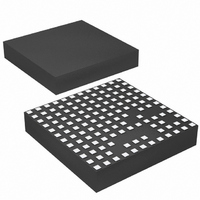
IC DC/DC UMODULE 12A 133-LGA
Manufacturer
Linear Technology
Series
µModuler
Type
Point of Load (POL) Non-Isolatedr
Datasheet
1.LTM4601AEVPBF.pdf
(28 pages)
Specifications of LTM4601AIV#PBF
Design Resources
LTM4601A Spice Model
Output
0.6 ~ 5 V
Number Of Outputs
1
Power (watts)
60W
Mounting Type
Surface Mount
Voltage - Input
4.5 ~ 20V
Package / Case
133-LGA
1st Output
0.6 ~ 5 VDC @ 12A
Size / Dimension
0.59" L x 0.59" W x 0.11" H (15mm x 15mm x 2.8mm)
Power (watts) - Rated
60W
Operating Temperature
-40°C ~ 85°C
Efficiency
95%
Dc To Dc Converter Type
Step Down
Pin Count
133
Input Voltage
20V
Output Voltage
0.6 to 5V
Switching Freq
850kHz
Output Current
12A
Package Type
LGA
Output Type
Adjustable
Switching Regulator
Yes
Load Regulation
1%
Line Regulation
0.3%
Mounting
Surface Mount
Input Voltage (min)
4.5V
Operating Temperature Classification
Industrial
Lead Free Status / RoHS Status
Lead free / RoHS Compliant
3rd Output
-
2nd Output
-
Lead Free Status / Rohs Status
Compliant
Available stocks
Company
Part Number
Manufacturer
Quantity
Price


APPLICATIONS INFORMATION
LTM4601A/LTM4601A-1
Run Enable
The RUN pin is used to enable the power module. The
pin has an internal 5.1V zener to ground. The pin can be
driven with a logic input not to exceed 5V.
The RUN pin can also be used as an undervoltage lockout
(UVLO) function by connecting a resistor divider from the
input supply to the RUN pin:
See Figure 1, Simplifi ed Block Diagram.
Power Good
The PGOOD pin is an open-drain pin that can be used to
monitor valid output voltage regulation. This pin monitors
a ±10% window around the regulation point and tracks
with margining.
COMP Pin
This pin is the external compensation pin. The module
has already been internally compensated for most output
voltages. Table 2 is provided for most application require-
ments. A spice model will be provided for other control
loop optimization.
PLLIN
The power module has a phase-locked loop comprised
of an internal voltage controlled oscillator and a phase
detector. This allows the internal top MOSFET turn-on
to be locked to the rising edge of the external clock. The
frequency range is ±30% around the operating frequency
of 850kHz. A pulse detection circuit is used to detect a
clock on the PLLIN pin to turn on the phase-lock loop.
The pulse width of the clock has to be at least 400ns and
2V in amplitude. During the start-up of the regulator, the
phase-lock loop function is disabled.
INTV
An internal low dropout regulator produces an internal
5V supply that powers the control circuitry and DRV
for driving the internal power MOSFETs. Therefore, if the
system does not have a 5V power rail, the LTM4601A
can be directly powered by V
14
V
UVLO
CC
and DRV
=
R1+ R2
R2
CC
Connection
• 1.5V
IN
. The gate driver current
CC
through the LDO is about 20mA. The internal LDO power
dissipation can be calculated as:
The LTM4601A also provides the external gate driver
voltage pin DRV
recommended to connect DRV
rail. This is especially true for higher input voltages. Do
not apply more than 6V to the DRV
be used to power the DRV
as shown in Figure 16.
Parallel Operation of the Module
The LTM4601A device is an inherently current mode
controlled device. Parallel modules will have very good
current sharing. This will balance the thermals on the de-
sign. Figure 19 shows a schematic of the parallel design.
The voltage feedback equation changes with the variable
N as modules are paralleled:
N is the number of paralleled modules.
Figure 19 shows an LTM4601A and an LTM4601A-1 used
in a parallel design. The 2nd LTM4601A device does
not require the remote sense amplifi er, therefore, the
LTM4601A-1 device is used. An LTM4601A device can be
used without the diff amp. V
and the V
When using multiple LTM4601A-1 devices in parallel with
an LTM4601A, limit the number to fi ve for a total of six
modules in parallel.
Thermal Considerations and Output Current Derating
The power loss curves in Figures 7 and 8 can be used
in coordination with the load current derating curves in
Figures 9 to 14 for calculating an approximate θ
module with various heat sinking methods. Thermal models
are derived from several temperature measurements at
the bench and thermal modeling analysis. Thermal Ap-
plication Note 103 provides a detailed explanation of the
analysis for the thermal models and the derating curves.
P
V
LDO_LOSS
OUT
= 0.6V
OSNS
= 20mA • (V
–
can be tied to INTV
CC
60.4k
. If there is a 5V rail in the system, it is
N
R
SET
+ R
IN
SET
CC
– 5V)
OSNS
pin with an external circuit
CC
+
CC
CC
pin to the external 5V
can be tied to ground
. DIFFV
pin. A 5V output can
OUT
can fl oat.
JA
for the
4601afb
Related parts for LTM4601AIV#PBF
Image
Part Number
Description
Manufacturer
Datasheet
Request
R

Part Number:
Description:
Ultralow EMI 28VIN, 6A DC/DC ?Module Regulator
Manufacturer:
LINER [Linear Technology]
Datasheet:

Part Number:
Description:
IC DC/DC UMODULE 12A 133-LGA
Manufacturer:
Linear Technology
Datasheet:

Part Number:
Description:
IC DC/DC UMODULE 12A 133-LGA
Manufacturer:
Linear Technology
Datasheet:
Part Number:
Description:
IC DC/DC UMODULE 12A 133-LGA
Manufacturer:
Linear Technology
Datasheet:

Part Number:
Description:
CD ROM LINEARVIEW DATASHEETS
Manufacturer:
Linear Technology

Part Number:
Description:
Standalone Linear Li-Ion Battery Charger with Thermal Regulation in ThinSOT
Manufacturer:
Linear Technology Corporation
Datasheet:
Part Number:
Description:
Low noise, high frequency, 8th order linear phase lowpass filter
Manufacturer:
Linear Technology Corporation
Datasheet:
Part Number:
Description:
Manufacturer:
Linear Technology Corporation
Datasheet:
Part Number:
Description:
Manufacturer:
Linear Technology Corporation
Datasheet:
Part Number:
Description:
Manufacturer:
Linear Technology Corporation
Datasheet:
Part Number:
Description:
Manufacturer:
Linear Technology Corporation
Datasheet:
Part Number:
Description:
Manufacturer:
Linear Technology Corporation
Datasheet:
Part Number:
Description:
Manufacturer:
Linear Technology Corporation
Datasheet:
Part Number:
Description:
Manufacturer:
Linear Technology Corporation
Datasheet:
Part Number:
Description:
Dual and Quad, JFET Input Precision High Speed Op Amps
Manufacturer:
Linear Technology Corporation
Datasheet: