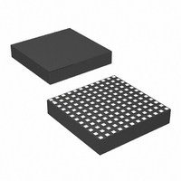
LTM4615IV#PBF Linear Technology, LTM4615IV#PBF Datasheet - Page 2

LTM4615IV#PBF
Manufacturer Part Number
LTM4615IV#PBF
Description
IC SWIT REG BUCK 4A ADJ 144LGA
Manufacturer
Linear Technology
Series
µModuler
Type
Point of Load (POL) Non-Isolatedr
Specifications of LTM4615IV#PBF
Design Resources
LTM4615 Spice Model
Output
0.8 ~ 5 V
Number Of Outputs
3
Power (watts)
12W
Mounting Type
Surface Mount
Voltage - Input
2.38 ~ 5.5 V
Package / Case
144-LGA
1st Output
0.8 ~ 5 VDC @ 4A
2nd Output
0.8 ~ 5 VDC @ 4A
3rd Output
0.8 ~ 5 VDC @ 4A
Size / Dimension
0.59" L x 0.59" W x 0.11" H (15mm x 15mm x 2.8mm)
Power (watts) - Rated
12W
Operating Temperature
-40°C ~ 125°C
Efficiency
95%
Primary Input Voltage
5.5V
No. Of Outputs
3
Output Voltage
5V
Output Current
1.5A
Voltage Regulator Case Style
LGA
No. Of Pins
144
Operating Temperature Range
-40°C To +125°C
Rohs Compliant
Yes
Dc To Dc Converter Type
Step Down
Pin Count
144
Input Voltage
5.5V
Switching Freq
1250KHz
Package Type
LGA
Output Type
Adjustable
Switching Regulator
Yes
Mounting
Surface Mount
Input Voltage (min)
2.375V
Operating Temperature Classification
Automotive
Lead Free Status / RoHS Status
Lead free / RoHS Compliant
Available stocks
Company
Part Number
Manufacturer
Quantity
Price
DEMO MANUAL DC1367A
QUICK START PROCEDURE
Demonstration circuit 1367A is an easy way to evaluate
the performance of the LTM4615. Please refer to Figure 1
for proper measurement equipment setup and follow the
procedure below:
1. Place jumpers in the following positions for a typical
2. With power off, preset the loads to 0A and V
3. Turn on the power at the input. The output voltage
+
–
2
V
1.8V, 1.2V and 1.0V application:
to be 5V. Connect the input power supply, load and
meters as shown in Figure 1.
between VO1+ and VO1– should be 1.8V ± 2%, the
voltage between VO2+ and VO2– should be 1.2V ± 2%,
and the voltage between VO3(LDO) and GND should be
1.0V ±2%.
0A TO
LOAD
4A
DISABLED
TRACK1
–
A
+
Figure 1. Test Setup of DC1367A
RUN1
–
–
ON
V
IN
V
+
–
+
+
A
+
A
0A TO
V
LOAD
–
+
1.5A
–
RUN2
ON
IN
supply
DC1376 F01
+
A
4. Once the proper output voltage is established, adjust
5. VOUT1 can track another supply by connecting TP14,
6. VOUT2 is used as the input supply for the 1.5A LDO.
7. Because DC1367A is designed so VOUT2 tracks VOUT1
8. VIN1 and VIN2 are shorted on DC1367A through a 1mΩ
–
the load within the operating range and observe the
output voltage regulation, ripple voltage, efficiency and
other parameters. To measure input and output ripple,
please refer to Figure 2 for proper setup.
TRACK to the supply rail and setting JP1 to ENABLED.
When R8 equals RSET1, VOUT1 is set up for coincidental
tracking. VOUT2 is set up to coincidentally track VOUT1
as determined by resistors R6 and R7. Please refer to
the circuit schematic and data sheet.
Therefore, if the jumper of JP3 (RUN2) is placed at OFF
position, both channel 2 and 3 will be turned off.
automatically, placing the JP2 (RUN1) to OFF position
turns off all three outputs. To disable tracking on VOUT2,
please remove R6 and R7 and connect TRACK2 to VIN2.
resistor, R10. If desired, remove R10 to allow separate
V
0A TO
LOAD
2.5A
Figure 2. Proper Scope Probe Placement for Measuring
Input or Output Ripple
IN1
and V
V
+
–
IN2
INPUT OR OUTPUT CAPACITOR
power supplies.
+
–
DC1376 F02
dc1367af


