LMZ12001TZE-ADJ/NOPB National Semiconductor, LMZ12001TZE-ADJ/NOPB Datasheet
LMZ12001TZE-ADJ/NOPB
Specifications of LMZ12001TZE-ADJ/NOPB
Available stocks


Related parts for LMZ12001TZE-ADJ/NOPB


LMZ12001TZE-ADJ/NOPB Summary of contents
Page 1
... Point of load conversions from 5V and 12V input rail ■ Time critical projects ■ Space constrained high thermal requirement applications ■ Negative output voltage applications (See AN-2027) © 2010 National Semiconductor Corporation LMZ12001 Performance Benefits ■ Operates at high ambient temperature with no thermal derating ■ ...
Page 2
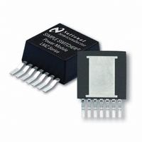
... Simplified Application Schematic Connection Diagram Ordering Information Order Number LMZ12001TZ-ADJ LMZ12001TZX-ADJ LMZ12001TZE-ADJ Pin Descriptions Pin Name Description 1 VIN Supply input — Nominal operating range is 4.5V to 20V . A small amount of internal capacitance is contained within the package assembly. Additional external input capacitance is required between this pin and exposed pad. ...
Page 3
Pin Name Description 6 FB Feedback — Internally connected to the regulation, over-voltage, and short-circuit comparators. The regulation reference point is 0.8V at this input pin. Connected the feedback resistor divider between the output and ground to set the output ...
Page 4
... Absolute Maximum Ratings If Military/Aerospace specified devices are required, please contact the National Semiconductor Sales Office/ Distributors for availability and specifications. VIN, RON to GND EN, FB GND Junction Temperature Storage Temperature Range Electrical Characteristics junction temperature (T ) range of -40°C to +125°C. Minimum and Maximum limits are guaranteed through test, design or statistical J correlation ...
Page 5
Symbol Parameter ΔV /ΔV Load Regulation O IN η Efficiency Note 1: Absolute Maximum Ratings are limits beyond which damage to the device may occur. Operating Ratings are conditions under which operation of the device is intended to be functional. ...
Page 6
Efficiency 6V Input @ 25°C Efficiency 8V Input @ 25°C Efficiency 12V Input @ 25°C www.national.com Dissipation 6V Input @ 25°C 30114821 Dissipation 8V Input @ 25°C 30114855 Dissipation 12V Input @ 25°C 30114803 6 30114822 30114856 30114804 ...
Page 7
Efficiency 20V Input @ 25°C 30114857 Efficiency 4.5V Input @ 85°C 30114859 Efficiency 5V Input @ 85°C 30114861 Dissipation 20V Input @ 25°C Dissipation 4.5V Input @ 85°C Dissipation 5V Input @ 85°C 7 30114858 30114860 30114862 www.national.com ...
Page 8
Efficiency 6V Input @ 85°C Efficiency 8V Input @ 85°C Efficiency 12V Input @ 85°C www.national.com Dissipation 6V Input @ 85°C 30114833 Dissipation 8V Input @ 85°C 30114840 Dissipation 12V Input @ 85°C 30114842 8 30114834 30114841 30114843 ...
Page 9
Efficiency 20V Input @ 85°C 30114863 Line and Load Regulation @ 25°C 30114848 Output Ripple 12V 3. 30114805 Dissipation 20V Input @ 85°C Line and Load Regulation @ 85°C Transient Response 12V 3.3V 0. Step ...
Page 10
Current Limit 1.8V Current Limit 3.3V Application Block Diagram www.national.com @25°C OUT 30114865 @85°C OUT 30114868 10 Current Limit 3.3V @25°C OUT 30114867 Thermal Derating V = 1.8V OUT 30114866 30114808 ...
Page 11
General Description The LMZ12001 SIMPLE SWITCHER® power module is an easy-to-use step-down DC-DC solution capable of driving load with exceptional power conversion efficiency, line and load regulation, and output accuracy. The LMZ12001 is available in an innovative ...
Page 12
SS pin. Voltage levels between 0.8V and 3.8V have no effect on other circuit operation. Note that the following conditions will reset the soft-start capacitor by discharging the SS input to ground ...
Page 13
Following is a comparison pair of waveforms of the showing both CCM (upper) and DCM operating modes. CCM and DCM Operating Modes V = 12V 3.3V 1A/0.25A The approximate formula for determining the ...
Page 14
Minimize trace length to the FB pin. Both feedback resistors, R and R FBT capacitor C , should be located close to the FB pin. Since FF the FB node is high impedance, maintain the copper area as small ...
Page 15
... ENT R 11.8 kΩ ENB C 22 nF, ±10%, X7R, 16V nF, ±10%, X7R, 16V SS D1 5.1V Case Size Case Size TO-PMOD-7 National Semiconductor 1206 Taiyo Yuden 1210 Taiyo Yuden 1206 Taiyo Yuden 1210 Taiyo Yuden 0603 Vishay Dale 0603 Vishay Dale 0603 Vishay Dale ...
Page 16
FIGURE 1. Top and bottom view of evaluation PCB 16 30114816 30114817 ...
Page 17
Physical Dimensions inches (millimeters) unless otherwise noted 7-Lead TZA Package NS Package Number TZA07A 17 www.national.com ...
Page 18
... For more National Semiconductor product information and proven design tools, visit the following Web sites at: www.national.com Products Amplifiers www.national.com/amplifiers Audio www.national.com/audio Clock and Timing www.national.com/timing Data Converters www.national.com/adc Interface www.national.com/interface LVDS www.national.com/lvds Power Management www.national.com/power Switching Regulators www.national.com/switchers LDOs www.national.com/ldo LED Lighting www ...