QF4A512-PA Quickfilter Technologies LLC, QF4A512-PA Datasheet - Page 7
QF4A512-PA
Manufacturer Part Number
QF4A512-PA
Description
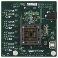
ADAPTER PROG FOR QF4A512-DK
Manufacturer
Quickfilter Technologies LLC
Specifications of QF4A512-PA
Accessory Type
Programming Adapter
For Use With/related Products
QF4A512-DK
For Use With
686-1004 - KIT DEV FOR QF4A512
Lead Free Status / RoHS Status
Contains lead / RoHS non-compliant
Other names
686-1005


7) Auto configure and Auto Start options:
8) Using an external clock source:
9) List of Test Point Definitions:
Rev A1, July 06
Step 12: Select “Download Image from File to EEPROM” in the software, when complete repeat Step 9 to Step 12
Recall that the QF4A512 can have auto configure and auto start set. If this occurs on either the QF4A512 – PA board
with a part in the socket, or on the QF4A512 part on the main development board, a conflict can occur at power up.
This can be solved by simply “resetting” the chip by pressing the “Reset Chip” Button on the configuration screen.
Since the crystal is lightly loaded, an external driving clock source can directly run the internal PLL.
You do not need to remove the 1 Meg resistor, crystal or 18 pF loading capacitors from the development board.
Simply apply the external clock source to Test Point TP22. Make sure to tell the Quickfilter software the external
clock frequency used when regenerating the QFP file.
TP1 = +5V from DC wall adapter.
TP2 = +3.3V from on board regulator.
TP3 = +1.8V from on board regulator.
TP22 = External clock input.
GND = Ground point for external clock and voltage measurement.
for each programmed part.
Programmers note – In many cases the QF4A512 parts are programmed with auto
configure and auto start enabled. However if the power is cycled, or the programmed part
is put back in the socket, the QF4A512 will start running and need to be stopped in order to
re-program it.
Designer’s note – The allowable input range is 5 MHz to 200 MHz.
The clock input on Pin 22 to the phase lock loop is a 1.8 Volt level. Therefore the amplitude
of the incoming clock source should be 1.62 to 1.98 Volts Peak to peak. Since the input is
AC coupled, a DC offset can exist. The clock can be a sine wave, or square wave.
Programming Adapter User’s Guide
7
www.quickfiltertech.com
QF4A512-PA
Related parts for QF4A512-PA
Image
Part Number
Description
Manufacturer
Datasheet
Request
R

Part Number:
Description:
KIT DEV FOR QF4A512
Manufacturer:
Quickfilter Technologies LLC
Datasheet:

Part Number:
Description:
KIT DEV FOR QF1F512
Manufacturer:
Quickfilter Technologies LLC
Datasheet:

Part Number:
Description:
KIT DEV FOR QF1DA512
Manufacturer:
Quickfilter Technologies LLC
Datasheet:

Part Number:
Description:
DEV KIT QF1D512 AUDIO MOJO
Manufacturer:
Quickfilter Technologies LLC

Part Number:
Description:
IC PROG SIGNAL CONV 4CH 32LQFP
Manufacturer:
Quickfilter Technologies LLC

Part Number:
Description:
IC FILTER DGTL PROGBL 16-VQFN
Manufacturer:
Quickfilter Technologies LLC
Datasheet:

Part Number:
Description:
IC SAVFIRE DGTL FILTER 1CH 16QFN
Manufacturer:
Quickfilter Technologies LLC

Part Number:
Description:
ADAPTER PROTOTYPING FOR QF1D512
Manufacturer:
Quickfilter Technologies LLC
Datasheet:

Part Number:
Description:
BOARD MSP-MOJO + EXPANSION HEADR
Manufacturer:
Quickfilter Technologies LLC
Datasheet:

Part Number:
Description:
REF DESIGN BLUETOOTH STER HDSET
Manufacturer:
Quickfilter Technologies LLC
Datasheet:
Part Number:
Description:
IC PROG SIGNAL CONV 4CH 32LQFP
Manufacturer:
Quickfilter Technologies LLC
Part Number:
Description:
IC FILTER DGTL PROGBL 16-VQFN
Manufacturer:
Quickfilter Technologies LLC
Datasheet:
Part Number:
Description:
IC SAVFIRE DGTL FILTER 1CH 16QFN
Manufacturer:
Quickfilter Technologies LLC