ATF15XXDK3-SAJ44 Atmel, ATF15XXDK3-SAJ44 Datasheet - Page 17
ATF15XXDK3-SAJ44
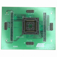
Manufacturer Part Number
ATF15XXDK3-SAJ44
Description
ADAPTER SKT ATF15XXBE 84/44PLCC
Manufacturer
Atmel
Datasheet
1.ATF15XXDK3-SAJ44.pdf
(44 pages)
Specifications of ATF15XXDK3-SAJ44
Module/board Type
Socket Module - PLCC
For Use With/related Products
ATF15xxDK3
Lead Free Status / RoHS Status
Contains lead / RoHS non-compliant


3605B–PLD–05/06
Hardware Description
2.1.6
2.1.7
2.1.8
2.1.9
2.1.10
2-10
VCCIO and VCCINT
Voltage Selection
Jumpers and LEDs
ICCIO and ICCINT
Jumpers
Voltage Regulators
Power Supply
Switch and Power
LED
Power Supply Jack
and Power Supply
Header
Table 2-14. Pin Numbers of GCLK1 and GCLK2
The VCCIO and VCCINT Voltage Selection Jumpers, labeled VCCIO Selector and
VCCINT Selector respectively on ATF15xx-DK3 Development/Programming Board,
allow the designers to select I/O supply voltage level (VCCIO) and core supply voltage
level (VCCINT) that are used for the target CPLD on the board. Once these jumpers are
set correctly, the LEDs (labeled VCCINT LED and VCCIO LED) will be turn on as
expected. However, at lower supply voltage levels (i.e. 2.5V or lower), the LEDs might
be very dim.
For ATF15xxAS/ASL (5.0V) CPLDs, both the VCCIO Selector and VCCINT Selector
jumpers MUST BE set to 5.0V. For ATF15xxASV/ASVL (3.3V) CPLDs, both the VCCIO
Selector and VCCINT Selector Jumpers MUST BE set to 3.3V only. For the ATF15xxBE
(1.8V) CPLDs, designers MUST SET VCCINT Selector jumper to 1.8V for its core volt-
age supply. However, designers can set the VCCIO Selector jumper to 3.3V, 2.5V, or
1.8V (but not 5.0V) in order for the I/Os of the ATF15xxBE CPLD to interface with differ-
ent voltage levels devices.
Note:
The IccIO and IccINT jumpers can be removed and used as Icc measurement points.
When the jumpers are removed, current meters can be connected to the posts to mea-
sure the current consumption of the target CPLD. When users are not using these
jumpers to measure the current, these jumpers must be set in order for the board and
CPLD to operate.
Two voltage regulators, labeled VR1 and VR2, are used to independently generate and
regulate the VCCINT and VCCIO voltages from the 9V DC power supply. For details,
please review the schematic of the ATF15xx-DK3 board.
The Power Supply Switch, labeled POWER SWITCH, can be switched to the ON or
OFF position, which is used to turn on or off the power of the ATF15xx-DK3 board
respectively. It allows the 9V DC voltage at the Power Supply Jack to pass to the volt-
age regulators when it is in the ON position. When the Power Supply Switch is turned
ON, the Power LED (labeled POWER LED) will light up to indicate that the ATF15xx-
DK3 board is supplied with power.
The Atmel ATF15xx-DK3 Development/Programmer Board contains two different types
of power supply connectors labeled JPower and JP Power. Either one of these power
supply connectors can be used to connect a 9V DC power source to the board. The first
power connector, labeled JPower, is a barrel power jack with a 2.1mm diameter post
and it mates to a 2.1mm (inner diameter) x 5.5mm (outer diameter) female plug. The
second is the power supply header, labeled JP Power, is a 4-pin male 0.1" header with
0.025" square posts. The availability of these two types of power connectors allows the
users to choose the type of power supply equipment to use for ATF15xx-DK3 Develop-
ment/Programmer Board. However, please note that only one of these two power
supply connectors should be powered with a 9V DC source but not both at the same
time.
GCLK1
GCLK2
The power of the CPLD Development/Programmer Board MUST BE turned
OFF when changing the position of the VCCIO or VCCINT voltage selection
jumper (VCCIO Selector or VCCINT Selector).
44-pin
TQFP
37
40
44-pin
PLCC
43
2
ATF15xx-DK3 Development Kit User Guide
84-pin
PLCC
83
2
100-pin
TQFP
87
90
Related parts for ATF15XXDK3-SAJ44
Image
Part Number
Description
Manufacturer
Datasheet
Request
R

Part Number:
Description:
ADAPTER SKT ATF15XXB PLCC/TQFP
Manufacturer:
Atmel
Datasheet:

Part Number:
Description:
ADAPTER SKT ATF15XXBE 84/84PLCC
Manufacturer:
Atmel
Datasheet:

Part Number:
Description:
KIT DEV 20TSSOP ADAPTER ATF15XX
Manufacturer:
Atmel
Datasheet:

Part Number:
Description:
KIT DEV FOR ATF15XX CPLD'S
Manufacturer:
Atmel
Datasheet:
Part Number:
Description:
ADAPTER FOR ATF15XX-DK2 44TQFP
Manufacturer:
Atmel
Datasheet:
Part Number:
Description:
ADAPTER FOR ATF15XX-DK2 44PLCC
Manufacturer:
Atmel
Datasheet:
Part Number:
Description:
ADAPTER FOR ATF15XX-DK2 68PLCC
Manufacturer:
Atmel
Datasheet:
Part Number:
Description:
ADAPTER FOR ATF15XX-DK2 100TQFP
Manufacturer:
Atmel
Datasheet:

Part Number:
Description:
IC TRANS E-PHEMT 2GHZ SOT-343
Manufacturer:
Avago Technologies US Inc.
Datasheet:
Part Number:
Description:
IC TRANS E-PHEMT 2GHZ SOT-343
Manufacturer:
Avago Technologies US Inc.
Datasheet:

Part Number:
Description:
TRANSISTOR,HEMT,N-CHAN,5.5V V(BR)DSS,175mA I(DSS),SOT-343R
Manufacturer:
Avago Technologies US Inc.
Part Number:
Description:
TRANSISTOR,HEMT,N-CHAN,3V V(BR)DSS,15mA I(DSS),SOT-363
Manufacturer:
Avago Technologies US Inc.
Datasheet:
Part Number:
Description:
TRANSISTOR,HEMT,N-CHAN,4.5V V(BR)DSS,90mA I(DSS),SOT-343R
Manufacturer:
Avago Technologies US Inc.
Datasheet: