EVB-USB2240-IND SMSC, EVB-USB2240-IND Datasheet - Page 5
EVB-USB2240-IND
Manufacturer Part Number
EVB-USB2240-IND
Description
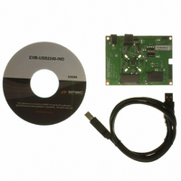
EVALUATION BOARD USB2241-AEZG
Manufacturer
SMSC
Specifications of EVB-USB2240-IND
Main Purpose
Memory, SD/MMC
Embedded
No
Utilized Ic / Part
USB2241
Primary Attributes
Read and Write to Over 22 Flash Media Formats from xD, MS, SD, and MMC
Secondary Attributes
Socket for External EEPROM Expansion, USB Power with 3.3 V Regulator
Interface Type
USB
Product
Interface Modules
Lead Free Status / RoHS Status
Lead free / RoHS Compliant
For Use With/related Products
USB2240
Other names
638-1078


EVB-USB2240-IND User Manual Revision B
SMSC EVB-USB2240-IND
2.1.8
Layout Considerations
The EVB-USB2240-IND is designed on four PCB layers: two signal layers and two supply layers. The
PCB layer stack is shown in
layers are ground and power. Note that the media I/F signals flow easily to their destination connectors
simplifying routing of critical signals.
The component side top layer is shown in
locations. Solder side and bottom layer is shown in
Component Side
Solder mask
Solder mask
Solder Side
Pre-preg
Pre-preg
Layer 1
Layer 2
Layer 3
Layer 4
Core
Figure 2.1 USBDM Configuration Interface
Table
Table 2.3 PCB layer stack
USER MANUAL
2.3. All signals are routed on top and bottom layers. The internal
Figure 2.2
5
4.25 mil, +/- 0.25 mil FR-4
4.25 mil, +/- 0.25 mil FR-4
1.8 - 3.1 mil, finished
1.8 - 3.1 mil, finished
1.3 mil (nominal)
1.3 mil (nominal)
~28 mil FR-4
Figure
with silk screen information to identify component
2.3.
Revision 1.0 (07-17-09)
Related parts for EVB-USB2240-IND
Image
Part Number
Description
Manufacturer
Datasheet
Request
R

Part Number:
Description:
ZIGBEE EVAL BOARD COORDINATOR-US
Manufacturer:
Laird Technologies
Part Number:
Description:
ZIGBEE EVAL BOARD COORDINATOR-US
Manufacturer:
Laird Technologies

Part Number:
Description:
ZIGBEE EVAL BOARD COORDINATOR-US
Manufacturer:
Laird Technologies

Part Number:
Description:
ZIGBEE EVAL BOARD COORDINATOR-US
Manufacturer:
Laird Technologies

Part Number:
Description:
FAST ETHERNET PHYSICAL LAYER DEVICE
Manufacturer:
SMSC Corporation
Datasheet:
Part Number:
Description:
357-036-542-201 CARDEDGE 36POS DL .156 BLK LOPRO
Manufacturer:
SMSC Corporation
Datasheet:
Part Number:
Description:
357-036-542-201 CARDEDGE 36POS DL .156 BLK LOPRO
Manufacturer:
SMSC Corporation
Datasheet:
Part Number:
Description:
357-036-542-201 CARDEDGE 36POS DL .156 BLK LOPRO
Manufacturer:
SMSC Corporation
Datasheet:
Part Number:
Description:
4-PORT USB2.0 HUB CONTROLLER
Manufacturer:
SMSC Corporation
Datasheet:
Part Number:
Description:
Manufacturer:
SMSC Corporation
Datasheet:
Part Number:
Description:
Manufacturer:
SMSC Corporation
Datasheet:
Part Number:
Description:
FDC37C672ENHANCED SUPER I/O CONTROLLER WITH FAST IR
Manufacturer:
SMSC Corporation
Datasheet:
Part Number:
Description:
COM90C66LJPARCNET Controller/Transceiver with AT Interface and On-Chip RAM
Manufacturer:
SMSC Corporation
Datasheet:
Part Number:
Description:
Manufacturer:
SMSC Corporation
Datasheet: