MCP46XXDM-PTPLS Microchip Technology, MCP46XXDM-PTPLS Datasheet - Page 22
MCP46XXDM-PTPLS
Manufacturer Part Number
MCP46XXDM-PTPLS
Description
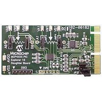
BOARD PICTAIL DIGI POT MCP4XXX
Manufacturer
Microchip Technology
Series
PICtail™ Plusr
Datasheet
1.MCP46XXDM-PTPLS.pdf
(44 pages)
Specifications of MCP46XXDM-PTPLS
Main Purpose
Digital Potentiometer
Embedded
No
Utilized Ic / Part
MCP46xx
Primary Attributes
1 Dual Pot, 10k Ohms, 257 Taps, I²C Interface
Secondary Attributes
2.7 ~ 5.5 V, 150 ppm/°C
Silicon Manufacturer
Microchip
Silicon Core Number
MCP4631, MCP4632, MCP4641, MCP4642, MCP4651, MCP4652, MCP4661, MCP4662
Kit Contents
Board
Lead Free Status / RoHS Status
Lead free / RoHS Compliant


DS51804A-page 18
TABLE 2-2:
8
9
10
11
12
14
15
16
17
18
19
20
Note 1:
Step
Release the Explorer 16 Development Board’s
S3 push button.
Configure oscilloscope as follows:
• Time-base = 100 µs/Division
Depress the Explorer 16 Development Board’s
S6 push button.
Depress the Explorer 16 Development Board’s
S4 push button.
Use the S4 and S6 push buttons to configure
the Volatile Wiper 1 register to either near V
or near V
Configure Scope to Capture on Channel 2.
Depress the Explorer 16 Development Board’s
S5 push button.
Unplug Power from the Explorer 16
Development Board.
Depress the Explorer 16 Development Board’s
S3 push button.
Power up the programmed Explorer 16
Development Board and depress and release
the MCLR push button.
Release the Explorer 16 Development Board’s
S3 push button.
Unplug Power from the Explorer 16
Development Board and remove the
MCP46XXDM-PTPLS board.
(see
The SDA and SCL signals go from V
operating at 3.3V. The VW1 signals go from V
Figure 2-7
SS
DEMO STEPS USING THE PICDEM HPC EXPLORER DEMO
BOARD (CONTINUED)
. Take note of Wiper Voltage value.
for scope details)
Action
SS
to approximately 3.3V due to the PIC24
DD
Program 2 is now selected.
—
While S6 is depressed, the voltage
on Wiper 1 (VW1) increases.
While S4 is depressed, the voltage
on Wiper 1 (VW1) decreases.
—
—
While S5 is depressed, the volatile
Wiper 1 register is read, this value is
written to the Non-Volatile Wiper 1
register, and then approximately a
10 ms delay occurs while the NV
write cycle occurs. Capture will look
similar to
—
—
—
The voltage on the Wiper 1 pad
(VW1) should be the same voltage
level as when Step 12 is completed.
—
SS
to approximately 5V.
© 2009 Microchip Technology Inc.
Figure 2-7
Result
. (Note 1)
Related parts for MCP46XXDM-PTPLS
Image
Part Number
Description
Manufacturer
Datasheet
Request
R

Part Number:
Description:
Manufacturer:
Microchip Technology Inc.
Datasheet:
Part Number:
Description:
Manufacturer:
Microchip Technology Inc.
Datasheet:
Part Number:
Description:
Manufacturer:
Microchip Technology Inc.
Datasheet:
Part Number:
Description:
Manufacturer:
Microchip Technology Inc.
Datasheet:
Part Number:
Description:
Manufacturer:
Microchip Technology Inc.
Datasheet:
Part Number:
Description:
Manufacturer:
Microchip Technology Inc.
Datasheet:
Part Number:
Description:
Manufacturer:
Microchip Technology Inc.
Datasheet:
Part Number:
Description:
Manufacturer:
Microchip Technology Inc.
Datasheet: