MCP1630RD-DDBK3 Microchip Technology, MCP1630RD-DDBK3 Datasheet - Page 6
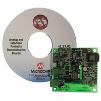
MCP1630RD-DDBK3
Manufacturer Part Number
MCP1630RD-DDBK3
Description
REF DESIGN MCP1630V BI-DIR 4CELL
Manufacturer
Microchip Technology
Type
Battery Managementr
Specifications of MCP1630RD-DDBK3
Main Purpose
Power Management, Battery Charger
Embedded
Yes, MCU, 8-Bit
Utilized Ic / Part
MCP1630
Primary Attributes
4 Cells- Li-Ion, 6.5 ~ 7 V Input
Secondary Attributes
MCU Generates Frequency, 94% Efficiency, 2 Status LEDs
Input Voltage
6.5 V to 7 V
Product
Power Management Modules
For Use With/related Products
MCP1630V, PIC16F88, MCP6022
Lead Free Status / RoHS Status
Not applicable / Not applicable
Lead Free Status / RoHS Status
Lead free / RoHS Compliant, Not applicable / Not applicable


MCP1630/MCP1630V
1.0
Absolute Maximum Ratings †
V
Maximum Voltage on Any Pin .. (V
V
Storage temperature .....................................-65°C to +150°C
Maximum Junction Temperature, T
Continuous Operating Temperature Range ..-40°C to +125°C
ESD protection on all pins, HBM
AC/DC CHARACTERISTICS
DS21896B-page 6
Electrical Specifications: Unless otherwise noted, V
V
Input Voltage
Input Operating Voltage
Input Quiescent Current
Oscillator Input
External Oscillator Range
Min. Oscillator High Time
Min. Oscillator Low Time
Oscillator Rise Time
Oscillator Fall Time
Oscillator Input Voltage Low
Oscillator Input Voltage High
Oscillator Input Capacitance
External Reference Input
Reference Voltage Input
Error Amplifier
Input Offset Voltage
Error Amplifier PSRR
Common Mode Input Range
Common Mode Rejection Ratio
Open-loop Voltage Gain
Low-level Output
Gain Bandwidth Product
Error Amplifier Sink Current
Error Amplifier Source Current
Note 1:
DD
EXT
IN
...................................................................................6.0V
for typical values = 5.0V, T
Short Circuit Current ...........................Internally Limited
2:
3:
ELECTRICAL
CHARACTERISTICS
Parameters
Capable of higher frequency operation depending on minimum and maximum duty cycles needed.
External oscillator input (OSC IN) rise and fall times between 10 ns and 10 µs used for characterization testing. Signal
levels between 0.8V and 2.0V with rise and fall times measured between 10% and 90% of maximum and minimum
values. Not production tested.
The reference input of the internal amplifier is capable of rail-to-rail operation.
A
= -40°C to +125°C.
GND
J
........................... +150°C
T
T
OH_MIN
OL_MIN
I
GBWP
SOURCE
PSRR
- 0.3)V to (V
I(V
T
T
C
F
V
Sym
A
I
V
V
V
SINK
V
RISE
FALL
V
OSC
V
OSC
REF
VOL
CM
OS
OL
IN
IN
H
L
)
GND - 0.3
IN
0.01
0.01
Min
3.0
2.0
80
85
—
—
—
—
—
—
—
+ 0.3)V
-4
-2
0
5
IN
3 kV
= 3.0V to 5.5V, F
Typ
2.8
0.1
3.5
—
—
10
—
—
—
—
—
99
—
80
95
25
11
-9
5
† Notice: Stresses above those listed under “Maximum
Ratings” may cause permanent damage to the device. This is
a stress rating only and functional operation of the device at
those or any other conditions above those indicated in the
operational listings of this specification is not implied.
Exposure to maximum rating conditions for extended periods
may affect device reliability.
AC/
GND + 50
OSC
Max
V
V
5.5
4.5
0.8
10
10
+4
—
—
—
—
—
—
—
1
IN
IN
= 1 MHz with 10% Duty Cycle, C
Units
MHz
MHz
mA
mV
mV
mA
mA
dB
dB
dB
ns
µs
µs
pf
V
V
V
V
V
V
V
I
Note 1
Note 2
Note 2
Note 2, Note 3
Note 2, Note 3
R
< V
RL = 5 k
V
V
V
V
V
EXT
IN
IN
IN
IN
COMP
IN
COMP
L
= 5 k to V
IN
© 2005 Microchip Technology Inc.
= 3.0V to 5.0V, V
= 5V, V
= 5V
= 5V, V
= 5V, V
= 0 mA, F
- 100 mV, V
= 2.0V
= 2.0V, Absolute Value
to V
CM
REF
REF
Conditions
IN
OSC IN
= 0V to 2.5V
IN
= 1.2V, V
= 1.2V, V
/2, 100 mV < V
IN
/2
CM
= 0.1 µF,
CM
= 1.2V
= 0 Hz
= 1.2V
FB
FB
= 1.4V,
= 1.0V,
EAOUT
Related parts for MCP1630RD-DDBK3
Image
Part Number
Description
Manufacturer
Datasheet
Request
R

Part Number:
Description:
REF DESIGN MCP1630 NIMH BATT CHG
Manufacturer:
Microchip Technology
Datasheet:

Part Number:
Description:
BOARD DEMO FOR MCP1630 LI-ION
Manufacturer:
Microchip Technology
Datasheet:

Part Number:
Description:
REFERENCE DESIGN FOR MCP1630
Manufacturer:
Microchip Technology
Datasheet:

Part Number:
Description:
MCP1630 Dual Synchronous Buck Regulator Demo Board DEVTOOL - Analog
Manufacturer:
Microchip Technology
Datasheet:
Part Number:
Description:
Power Management IC Development Tools MCP1630 Sepic Automotive LED Drvr
Manufacturer:
Microchip Technology
Datasheet:

Part Number:
Description:
Manufacturer:
Microchip Technology Inc.
Datasheet:
Part Number:
Description:
Manufacturer:
Microchip Technology Inc.
Datasheet:
Part Number:
Description:
Manufacturer:
Microchip Technology Inc.
Datasheet:
Part Number:
Description:
Manufacturer:
Microchip Technology Inc.
Datasheet:
Part Number:
Description:
Manufacturer:
Microchip Technology Inc.
Datasheet:
Part Number:
Description:
Manufacturer:
Microchip Technology Inc.
Datasheet: