EVL6563S-100W STMicroelectronics, EVL6563S-100W Datasheet - Page 4
EVL6563S-100W
Manufacturer Part Number
EVL6563S-100W
Description
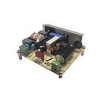
EVAL BOARD FOR L6563(100W)
Manufacturer
STMicroelectronics
Type
Power Factor Correctionr
Specifications of EVL6563S-100W
Main Purpose
Power Management, Power Factor Correction
Embedded
No
Utilized Ic / Part
L6563
Primary Attributes
100W Power Factor Correction and Preregulator Combination
Secondary Attributes
Transition Mode & Active Tracking Boost Function.
Board Size
90 mm x 83 mm
Maximum Operating Temperature
+ 60 C
Operating Supply Voltage
90 V to 265 V
Product
Power Management Modules
Dimensions
90 mm x 83 mm
Lead Free Status / RoHS Status
Lead free / RoHS Compliant
For Use With/related Products
L6563S
Other names
497-10490


Main characteristics and circuit description
1
4/33
Main characteristics and circuit description
The main characteristics of the SMPS are listed below:
●
●
●
●
●
●
●
●
●
●
This demonstration board implements a power factor correction (PFC) pre-regulator,100 W
continuous power, on a regulated 400 V rail from a wide-range mains voltage and provides
for the reduction of the mains harmonics, allowing to meet the European EN61000-3-2 or
the Japanese JEITA-MITI standard. The regulated output voltage is typically the input for the
cascaded isolated DC-DC converter that provides the output rails required by the load.
The board is designed to allow full-load operation in still air.
The power stage of the PFC is a conventional boost converter, connected to the output of
the rectifier bridge D1. It is completed by the coil L2, the diode D3 and the capacitor C6. The
boost switch is represented by the power MOSFET Q1. The NTC R1 limits the inrush
current at switch-on. It has been connected on the DC rail, in series to the output electrolytic
capacitor, in order to improve the efficiency during low line operation because the RMS
current flowing into the output stage is lower than current flowing into the input one at the
same input voltage, thus increasing efficiency. The board is equipped with an input EMI filter
necessary to filter the commutation noise coming from the boost stage.
At startup the L6563S is powered by the capacitor C11 that is charged via the resistors R7
and R16. Then the L2 secondary winding and the charge pump circuit (C7, R4, D4 and D5)
generate the Vcc voltage powering the L6563S during normal operation. The L2 secondary
winding is also connected to the L6563S pin #11 (ZCD) through the resistor R5. Its purpose
is supply the information that L2 has demagnetized, needed by the internal logic for
triggering a new switching cycle.
The divider R9, R12, R17 and R19 provides the L6563S multiplier with the information of the
instantaneous mains voltage that is used to modulate the peak current of the boost.
The resistors R2, R8, R10 with R13 and R14 are dedicated to sense the output voltage and
feed back to the L6563S the information necessary to regulate the output voltage. The
components C9, R18 and C8 constitute the error amplifier compensation network necessary
to keep the required loop stability.
The peak current is sensed by resistors R25 and R26 in series to the MOSFET and signal is
fed into pin #4 (CS) of the L6563S via the filter composed of R24 and C15.
C13, R27 and R32 connected to pin #5 (V
derives the information on the RMS mains voltage. The voltage signal at this pin, a DC level
equal to the peak voltage on pin #3 (MULT), is fed to a second input to the multiplier for the
Line voltage range: 90 to 265 Vac
Minimum line frequency (f
Regulated output voltage: 400 V
Rated output power: 100 W
Maximum 2f
Hold-up time: 10 ms (V
Minimum switching frequency: 40 kHz
Minimum estimated efficiency: 92% (at Vin = 90 Vac, Pout = 100 W)
Maximum ambient temperature: 50 °C
PCB type and size: single side, 35 µm, CEM-1, 90 x 83 mm
L
output voltage ripple: 20 V pk-pk
DROP
Doc ID 16279 Rev 2
L
): 47 Hz
after hold-up time: 300 V)
FF
) complete an internal peak-holding circuit that
AN3065
Related parts for EVL6563S-100W
Image
Part Number
Description
Manufacturer
Datasheet
Request
R

Part Number:
Description:
EVAL BOARD FOR L6563(250W)
Manufacturer:
STMicroelectronics
Datasheet:

Part Number:
Description:
EVAL BOARD FOR L6563(400W)
Manufacturer:
STMicroelectronics
Datasheet:

Part Number:
Description:
Power Management Modules & Development Tools Tranisition Mode PFC L6563S EVL Board
Manufacturer:
STMicroelectronics
Datasheet:

Part Number:
Description:
EVAL BOARD L6563 (200W)
Manufacturer:
STMicroelectronics
Datasheet:
Part Number:
Description:
STMicroelectronics [RIPPLE-CARRY BINARY COUNTER/DIVIDERS]
Manufacturer:
STMicroelectronics
Datasheet:
Part Number:
Description:
STMicroelectronics [LIQUID-CRYSTAL DISPLAY DRIVERS]
Manufacturer:
STMicroelectronics
Datasheet:

Part Number:
Description:
BOARD EVAL FOR MEMS SENSORS
Manufacturer:
STMicroelectronics
Datasheet:
Part Number:
Description:
NPN TRANSISTOR POWER MODULE
Manufacturer:
STMicroelectronics
Datasheet:
Part Number:
Description:
TURBOSWITCH ULTRA-FAST HIGH VOLTAGE DIODE
Manufacturer:
STMicroelectronics
Datasheet:
Part Number:
Description:
Manufacturer:
STMicroelectronics
Datasheet:
Part Number:
Description:
DIODE / SCR MODULE
Manufacturer:
STMicroelectronics
Datasheet:
Part Number:
Description:
DIODE / SCR MODULE
Manufacturer:
STMicroelectronics
Datasheet: