EVL6563S-250W STMicroelectronics, EVL6563S-250W Datasheet
EVL6563S-250W
Specifications of EVL6563S-250W
Available stocks


Related parts for EVL6563S-250W


EVL6563S-250W Summary of contents
Page 1
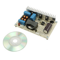
... W, wide-range mains input PFC pre-conditioner suitable for desktop PCs, industrial SMPS, flat screen displays, and all SMPS having to meet the IEC61000-3-2 or the JEITA-MITI standard. Figure 1. EVL6563S-250W: L6563S 250W TM PFC demonstration board November 2010 Application note Doc ID 16849 Rev 2 AN3119 1/32 www ...
Page 2
Contents Contents 1 Main characteristics and circuit description . . . . . . . . . . . . . . . . . . . . . 4 2 Electrical diagram . . . . . . . ...
Page 3
... EVL6563S-250W TM PFC: input current waveform @230 V- load . . . . . . . . 11 Figure 10. EVL6563S-250W TM PFC: input current waveform @100 V- load . . . . . . . . 11 Figure 11. EVL6563S-250W TM PFC: power factor vs. output power Figure 12. EVL6563S-250W TM PFC: THD vs. output power . . . . . . . . . . . . . . . . . . . . . . . . . . . . . . . 12 Figure 13. EVL6563S-250W TM PFC: efficiency vs. output power . . . . . . . . . . . . . . . . . . . . . . . . . . 12 Figure 14. EVL6563S-250W TM PFC: average efficiency acc Figure 15. ...
Page 4
Main characteristics and circuit description 1 Main characteristics and circuit description The main characteristics of the SMPS are: ● Line voltage range 265 Vac ● Line frequency (f ● Regulated output voltage: 400 V ● Rated output power: ...
Page 5
AN3119 the mains voltage. Additionally, pin #10 (RUN) is connected to pin and R28 resistor divider, providing a voltage level for brown-out (AC mains under voltage) protection. A voltage on the RUN pin below 0.8 V shuts down ...
Page 6
... Electrical diagram 2 Electrical diagram Figure 2. EVL6563S-250W TM PFC demonstration board: electrical schematic 6/32 Doc ID 16849 Rev 2 AN3119 ...
Page 7
... AN3119 3 Bill of material Table 1. EVL6563S-250W TM PFC demonstration board BOM Part type/ Case style Des. part value /package C1 470N-X2 6X26.5 mm C10 680N C11 2N2 C12 1 µF C13 2N2 C14 220 pF C15 2N2 C2 1 µF-X2 11X26 1.5 µF-520 V 12X26 100 µF - 450 V Dia. 18X35 mm 450 V, aluminium ELCAP, TXW series, 105 °C ...
Page 8
... Bill of material Table 1. EVL6563S-250W TM PFC demonstration board BOM (continued) Part type/ Case style Des. part value /package JPX4 Wire jumper JPX5 Wire jumper JPX6 Wire jumper JPX7 Wire jumper JPX8 Wire jumper L1 LH30-792Y3R0-01 L2 180 µH Q1 STF12NM50N TO-220FP Q2 STF12NM50N TO-220FP R1 NTC 1R0-S237 R10 27 kΩ ...
Page 9
... AN3119 Table 1. EVL6563S-250W TM PFC demonstration board BOM (continued) Part type/ Case style Des. part value /package 100 Ω R32 R33 51 kΩ R4 2.2 MΩ R5 150 kΩ MΩ MΩ R8 2.2 MΩ kΩ 0 Ω RX1 47 Ω RX3 0 Ω RX4 U1 L6563S Z1 PCB rev. 1 Description 0805 SMD STD film res - 1 250 ppm/° ...
Page 10
... Vin = 230 Vac - 50 Hz, Pout = 70 W, THD = 10. 0.869 10/32 Figure 4. EVL6563S-250W TM PFC: compliance to JEITA-MITI standard at 250 W Vin = 100 Vac - 50 Hz, Pout = 250 W, THD = 3. 0.999 Figure 6. EVL6563S-250W TM PFC: compliance to JEITA-MITI standard Vin = 100 Vac - 50 Hz, Pout = 70 W, THD = 5 0.995 Doc ID 16849 Rev 2 AN3119 ...
Page 11
... Test results and significant waveforms Figure 8. EVL6563S-250W TM PFC: input current waveform @100 V- 250 W load CH1: Vout CH2: V bridge CH4: I_AC Figure 10. EVL6563S-250W TM PFC: input current waveform @100 V- load CH1: Vout CH2: V bridge CH4: I_AC Figure 11 and 12. As shown, the PF remains close to unity ...
Page 12
... The average efficiency calculated according to the ES-2 requirements at different nominal mains voltages is shown in Figure 14. Figure 13. EVL6563S-250W TM PFC: efficiency vs. output power 12/32 Figure 12. EVL6563S-250W TM PFC: THD vs. output power Figure 13, measured according to the ES-2 Figure 14. EVL6563S-250W TM PFC: average efficiency acc. to ES-2 Doc ID 16849 Rev 2 AN3119 ...
Page 13
... AN3119 Figure 15. EVL6563S-250W TM PFC: static Vout regulation vs. output power The measured output voltage at different line and static load conditions is shown in Figure 15. As seen, the voltage is very stable over all the input voltage and output load range. 4.2 MOSFET current, TM signals, and L6563S THD optimizer In the following images the waveforms relevant to the switch current at 100 Vac voltage mains are shown ...
Page 14
... Vac - full load CH1: Q1 gate voltage, CH2: Q2 gate voltage CH3: Q1 drain current CH4: Q2 drain current , INV, and COMP pins are shown. FF Figure 19. EVL6563S-250W TM PFC: L6563S control pins-2 at 115 Vac - full load CH1: INV - pin #1, CH2: MULT - pin #3, CH3: COMP - pin #2 CH4 pin #5 ...
Page 15
... In Figure 21 the behavior of the EVL6563S-250W demonstration board in the case of an input voltage surge from 90 to 140 Vac is shown; in the image it is evident that the V function provides for the stability of the output voltage which is not affected by the input voltage surge ...
Page 16
... CH1: Vout, CH2: MULT (pin #3), CH4: I_AC 16/32 Figure 21. EVL6563S-250W TM PFC: input input CH1: Vout, CH3: V CH4: I_AC Figure 23. EVL6563S-250W TM PFC: input input CH1: Vout, CH2: MULT (pin #3), CH2: V CH4: I_AC Doc ID 16849 Rev 2 mains surge 90 Vac to 140 Vac (pin #5), CH2: MULT (pin #3) FF function ...
Page 17
... Test results and significant waveforms Figure 24 and Figure rd harmonic current distortion is not noticeable; this Figure 24 and 25: Figure 25. EVL6563S-250W TM PFC: input =390 kΩ FF THD= 2.94%, 3rd harmonic=30.5 mA CH2: MULT (pin #3) CH3: V (pin #5) FF CH4: I_AC Doc ID 16849 Rev 2 ...
Page 18
... Test results and significant waveforms Figure 26. EVL6563S-250W TM PFC: startup attempt at 80 Vac- full load In Figure 26 a startup tentative below the threshold is shown. As seen, at startup the RUN pin does not allow the PFC startup even if the Vcc has reached the turn-on threshold. PFC output voltage remains at the peak of the input sinewave ...
Page 19
... CH4: gate drive (pin #13) show the waveforms during the startup of the circuit at mains plug-in. 29 the waveforms during startup of the circuit at mains plug-in are shown. Figure 30. EVL6563S-250W TM PFC: startup at CH1: PFC output voltage CH2: Vcc voltage (pin #14) CH3: RUN (pin #10) CH4: gate drive (pin #13) ...
Page 20
... Figure output voltage exceeds a pre-set value (VOVP), usually larger than the maximum Vout that can be expected, also including worst-case load/line transients. For the EVL6563S-250W 400 V, Vovp = 434 V. Select: R21+R25+R26=8.8 MΩ; then: R33=8.8 MΩ·2.5/(434-2.5)=51 kΩ. Once this function is triggered, the gate drive activity is immediately stopped until the voltage on the PFC_OK pin drops below 2 ...
Page 21
... AN3119 Figure 31. EVL6563S-250W load transient at 115 Vac - full load to no-load The event of an open-loop is demonstrated in intervention, latching the operation of the L6563S. As mentioned previously, to restart the system it is necessary to recycle the input power. The connection of the startup resistors after the rectifier bridge allows a restart, in case of latch, faster than connecting the resistor to the bulk capacitor ...
Page 22
Test results and significant waveforms 4.6 TBO (tracking boost option) To achieve the TBO function on the L6563S a dedicated input of the multiplier is available on pin #6 (TBO); the function can be realized by simply connecting a resistor ...
Page 23
... The EVL6563S-250W offers the possibility to test these function by connecting it to the cascaded converter via the R30, R31, R32 series resistors. Regarding the PWM_STOP pin Test results and significant waveforms ...
Page 24
Test results and significant waveforms (#9), which is an open collector type needs a pull-up resistor please connect it close to the cascaded PWM for a better noise immunity. Figure 35. Interface circuits that let the L6563S switch ...
Page 25
... MULT dividers close to the L6563S pin #12 (GND). 7. Connect a ceramic capacitor (100÷470 nF) to pin #14 (Vcc) and pin #12 (GND), close to the L6563S. Connect this point to the RTN star point (see rule 1). Figure 37. EVL6563S-250W TM PFC: PCB layout (SMT side view) Doc ID 16849 Rev 2 Layout hints 25/32 ...
Page 26
Thermal map 6 Thermal map In order to check the design reliability, a thermal mapping by means camera was done. In Figure 38 input voltage, are shown. Some pointers visible in the image have been placed across ...
Page 27
AN3119 Table 2. Thermal maps reference points - PCB top side Point Reference R23 and R24 Doc ID 16849 Rev 2 Thermal map ...
Page 28
... TM control. Figure 40. EVL6563S-250W CE AVG measurement at 115 Vac- full load - phase wire 28/32 43 show the measurement in average mode of the conducted noise Figure 41. EVL6563S-250W CE AVG measurement at 115 Vac- full load - neutral wire Doc ID 16849 Rev 2 AN3119 ...
Page 29
... AN3119 Figure 42. EVL6563S-250W CE AVG measurement at 230 Vac- full load - phase wire EMI filtering and conducted EMI pre-compliance measurements Figure 43. EVL6563S-250W CE AVG measurement at 230 Vac- full load - neutral wire Doc ID 16849 Rev 2 29/32 ...
Page 30
References 8 References 1. L6563S datasheet 2. AN3027 “How to design a TM PFC pre-regulator with L6563S and L6563H” 30/32 Doc ID 16849 Rev 2 AN3119 ...
Page 31
AN3119 9 Revision history Table 3. Document revision history Date 29-Jun-2010 24-Nov-2010 Revision 1 Initial release. 2 Update Chapter 1 on page Doc ID 16849 Rev 2 Revision history Changes 4, Chapter 4.5 on page 20. 31/32 ...
Page 32
... Information in this document is provided solely in connection with ST products. STMicroelectronics NV and its subsidiaries (“ST”) reserve the right to make changes, corrections, modifications or improvements, to this document, and the products and services described herein at any time, without notice. All ST products are sold pursuant to ST’s terms and conditions of sale. ...