EVL6562A-400W STMicroelectronics, EVL6562A-400W Datasheet - Page 4
EVL6562A-400W
Manufacturer Part Number
EVL6562A-400W
Description
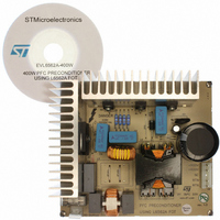
BOARD EVAL FOR L6562AX
Manufacturer
STMicroelectronics
Type
Power Factor Correctionr
Specifications of EVL6562A-400W
Main Purpose
Power Management, Power Factor Correction
Embedded
No
Utilized Ic / Part
L6562A
Primary Attributes
400W, 400V Out, 90 ~ 265VAC In
Secondary Attributes
Continuous Current Mode
Input Voltage
90 V to 265 V
Output Voltage
400 V
Board Size
1148.5 mm x 132 mm
Product
Power Management Modules
Dimensions
1148.5 mm x 132 mm
Lead Free Status / RoHS Status
Lead free / RoHS Compliant
For Use With/related Products
L6562A
Other names
497-8249
Available stocks
Company
Part Number
Manufacturer
Quantity
Price


Pin settings
2
2.1
2.2
4/26
Pin settings
Pin connection
Figure 2.
Pin description
Table 2. Pin description
Pin N°
1
2
3
4
5
6
7
8
COMP
Name
MULT
Pin connection (top view)
GND
ZCD
INV
Vcc
GD
CS
Inverting input of the error amplifier. The information on the output voltage of
the PFC pre-regulator is fed into this pin through a resistor divider. The pin
doubles as an ON/OFF control input.
Output of the error amplifier. A compensation network is placed between this
pin and INV to achieve stability of the voltage control loop and ensure high
power factor and low THD.
Main input to the multiplier. This pin is connected to the rectified mains
voltage via a resistor divider and provides the sinusoidal reference to the
current loop.
Input to the PWM comparator. The current flowing in the MOSFET is sensed
through a resistor, the resulting voltage is applied to this pin and compared
with an internal sinusoidal-shaped reference, generated by the multiplier, to
determine MOSFET’s turn-off. The pin is equipped with 200 ns leading-edge
blanking for improved noise immunity.
Boost inductor’s demagnetization sensing input for transition-mode
operation. A negative-going edge triggers MOSFET’s turn-on.
Ground. Current return for both the signal part of the IC and the gate driver.
Gate driver output. The totem pole output stage is able to drive power
MOSFET’s and IGBT’s with a peak current of 600 mA source and 800 mA
sink. The high-level voltage of this pin is clamped at about 12V to avoid
excessive gate voltages in case the pin is supplied with a high Vcc.
Supply Voltage of both the signal part of the IC and the gate driver. The
supply voltage upper limit is extended to 22V min. to provide more headroom
for supply voltage changes.
COMP
MULT
INV
CS
1
2
3
4
Description
8
7
6
5
Vcc
GD
GND
ZCD
L6562A
Related parts for EVL6562A-400W
Image
Part Number
Description
Manufacturer
Datasheet
Request
R

Part Number:
Description:
BOARD EVAL FOR L6562AX
Manufacturer:
STMicroelectronics
Datasheet:

Part Number:
Description:
BOARD EVAL FOR L6562A
Manufacturer:
STMicroelectronics
Datasheet:

Part Number:
Description:
EVALUATION MODULE L6562A
Manufacturer:
STMicroelectronics
Datasheet:

Part Number:
Description:
STMicroelectronics [RIPPLE-CARRY BINARY COUNTER/DIVIDERS]
Manufacturer:
STMicroelectronics
Datasheet:
Part Number:
Description:
STMicroelectronics [LIQUID-CRYSTAL DISPLAY DRIVERS]
Manufacturer:
STMicroelectronics
Datasheet:

Part Number:
Description:
BOARD EVAL FOR MEMS SENSORS
Manufacturer:
STMicroelectronics
Datasheet:
Part Number:
Description:
NPN TRANSISTOR POWER MODULE
Manufacturer:
STMicroelectronics
Datasheet:
Part Number:
Description:
TURBOSWITCH ULTRA-FAST HIGH VOLTAGE DIODE
Manufacturer:
STMicroelectronics
Datasheet:
Part Number:
Description:
Manufacturer:
STMicroelectronics
Datasheet:
Part Number:
Description:
DIODE / SCR MODULE
Manufacturer:
STMicroelectronics
Datasheet:
Part Number:
Description:
DIODE / SCR MODULE
Manufacturer:
STMicroelectronics
Datasheet:
Part Number:
Description:
Search -----> STE16N100
Manufacturer:
STMicroelectronics
Datasheet: