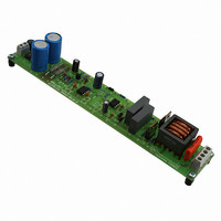
NCP5104BA36WGEVB ON Semiconductor, NCP5104BA36WGEVB Datasheet

NCP5104BA36WGEVB
Specifications of NCP5104BA36WGEVB
Related parts for NCP5104BA36WGEVB
NCP5104BA36WGEVB Summary of contents
Page 1
NCP5104 High Voltage, Half Bridge Driver The NCP5104 is a High Voltage Power gate Driver providing two outputs for direct drive of 2 N−channel power MOSFETs or IGBTs arranged in a half−bridge configuration. It uses the bootstrap technique to insure ...
Page 2
Vbulk C1 GND Vcc C3 1 GND Vcc 2 IN NCP1395 GND NCP5104 GND GND Figure 1. Typical Application Resonant Converter (LLC type) + Vbulk C1 GND Vcc C3 GND 1 Vcc SG3526 2 IN MC34025 ...
Page 3
PIN DESCRIPTION Pin Name Á Á Á Á Á Á Á Á Á Á Á Á Á Á Á Á Á Á Á Á Á IN Á Á Á Á Á Á Á Á Á Á Á Á ...
Page 4
ELECTRICAL CHARACTERISTIC (V Rating OUTPUT SECTION Output high short circuit pulsed current V DRV Output low short circuit pulsed current V DRV Output resistor (Typical value @ 25°C) Source Output resistor (Typical value @ 25°C) Sink High level output voltage, ...
Page 5
IN SD DRV_HI DRV_LO Note: DRV_HI output is in phase with the input 50% IN ton DRV_HI toff 90% DRV_LO 10% Figure 4. Input/Output Timing Diagram 50% tr toff 90% 90% Dead time 10% tf Ton = Toff + DT ...
Page 6
IN DeadTime1 DRV_HI toff_LO 90% Matching Delay1=toff_HI−toff_LO DRV_LO Matching Delay 2=(toff_LO+DT1)−(tof f _HI+DT2) Figure 6. Matching Propagation Delay Definition 50% SD DRV_HI DRV_LO Figure 7. Shutdown Waveform Definition 50% toff_HI 90% 10% DeadTime2 50% tsd_en tsd_dis 90% 10% http://onsemi.com ...
Page 7
T Low Side ON 650 600 550 T High Side ON 500 450 400 VOLTAGE (V) CC Figure 8. Turn ON Propagation Delay vs. Supply Voltage ( 160 ...
Page 8
Low Side r 120 100 80 t High Side VOLTAGE (V) CC Figure 14. Turn ON Risetime vs. Supply Voltage ( BOOT 80 ...
Page 9
V , VOLTAGE (V) CC Figure 20. Low Level Input Voltage Threshold vs. Supply Voltage (V CC 2.5 2.0 1.5 1.0 0 ...
Page 10
V , VOLTAGE (V) CC Figure 26. Logic “1” Input Current vs. Supply Voltage ( BOOT 1.0 0.8 0.6 0.4 0 ...
Page 11
I 350 src 300 250 200 150 100 VOLTAGE (V) CC Figure 32. Output Source Current vs. Supply Voltage ( BOOT 600 I High Side sink 500 I ...
Page 12
V , VOLTAGE (V) BOOT Figure 38. V Supply Current vs. Bootstrap BOOT Supply Voltage ( 240 200 160 120 4.0 8.0 12 ...
Page 13
nF LOAD 5.0 R GATE 0 0 100 200 300 400 SWITCHING FREQUENCY (kHz) Figure 44. I Consumption vs. Switching CC1 Frequency with 15 nC Load on Each Driver @ ...
Page 14
... G C SEATING PLANE −Z− 0.25 (0.010 *For additional information on our Pb−Free strategy and soldering details, please download the ON Semiconductor Soldering and Mounting Techniques Reference Manual, SOLDERRM/D. PACKAGE DIMENSIONS SOIC−8 NB CASE 751−07 ISSUE 0.10 (0.004 SOLDERING FOOTPRINT* 1 ...
Page 15
... SCILLC is an Equal Opportunity/Affirmative Action Employer. This literature is subject to all applicable copyright laws and is not for resale in any manner. PUBLICATION ORDERING INFORMATION LITERATURE FULFILLMENT: Literature Distribution Center for ON Semiconductor P.O. Box 5163, Denver, Colorado 80217 USA Phone: 303−675−2175 or 800−344−3860 Toll Free USA/Canada Fax: 303− ...


