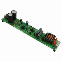
NCP5106BA36WGEVB ON Semiconductor, NCP5106BA36WGEVB Datasheet

NCP5106BA36WGEVB
Specifications of NCP5106BA36WGEVB
Related parts for NCP5106BA36WGEVB
NCP5106BA36WGEVB Summary of contents
Page 1
NCP5106A, NCP5106B High Voltage, High and Low Side Driver The NCP5106 is a high voltage gate driver IC providing two outputs for direct drive of 2 N−channel power MOSFETs or IGBTs arranged in a half−bridge configuration version B or any ...
Page 2
Vbulk C1 D4 GND Vcc GND VBOOT Vcc 2 IN_HI DRV_HI NCP1395 3 IN_LO 4 GND DRV_LO NCP5106 GND GND Figure 1. Typical Application Resonant Converter (LLC type) + Vbulk C1 D4 GND Vcc C3 U1 ...
Page 3
VCC VCC UV DETECT IN_HI GND IN_LO DELAY GND GND GND Figure 3. Detailed Block Diagram: Version A VCC VCC UV DETECT IN_HI CROSS GND CONDUCTION PREVENTION IN_LO GND Figure 4. Detailed Block Diagram: Version B PIN DESCRIPTION Pin Name ...
Page 4
MAXIMUM RATINGS Rating V Main power supply voltage CC V Main transient power supply voltage: CC_transient during 10 ms CC_max V VHV: High Voltage BRIDGE pin BRIDGE V Allowable Negative Bridge Pin Voltage for IN_LO Signal ...
Page 5
ELECTRICAL CHARACTERISTIC (V Rating OUTPUT SECTION Output high short circuit pulsed current V DRV Output low short circuit pulsed current V DRV Output resistor (Typical value @ 25°C) Source Output resistor (Typical value @ 25°C) Sink High level output voltage, ...
Page 6
IN_HI IN_LO DRV_HI DRV_LO Figure 5. Input/Output Timing Diagram (A Version) IN_HI IN_LO DRV_HI DRV_LO Figure 6. Input/Output Timing Diagram (B Version) 50% IN_HI (IN_LO DRV_HI (DRV_LO) 10% Figure 7. Propagation Delay and Rise / Fall ...
Page 7
IN_LO & 50% IN_HI ton_HI Delta_t DRV_HI ton_LO DRV_LO 10% Figure 8. Matching Propagation Delay (A Version) 50% IN_HI ton_HI DRV_HI 50% IN_LO toff_LO 90% DRV_LO Figure 9. Matching Propagation Delay (B Version) 50% toff_HI 90% 10% toff_LO Matching Delay ...
Page 8
IN_HI IN_LO DRV_HI DRV_LO Internal Deadtime Figure 10. Input/Output Cross Conduction Output Protection Timing Diagram (B Version) http://onsemi.com 8 Internal Deadtime ...
Page 9
T High Side ON 100 Low Side VOLTAGE (V) CC Figure 11. Turn ON Propagation Delay vs. Supply Voltage ( 140 120 ...
Page 10
Low Side VOLTAGE (V) CC Figure 17. Turn ON Risetime vs. Supply Voltage ( BOOT Low ...
Page 11
V , VOLTAGE (V) CC Figure 23. Low Level Input Voltage Threshold vs. Supply Voltage (V 2.5 2 1 ...
Page 12
V , VOLTAGE (V) CC Figure 29. Logic “1” Input Current vs. Supply Voltage ( BOOT 1 0.8 0.6 0.4 0 ...
Page 13
I High Side src 300 250 I src 200 150 100 VOLTAGE (V) CC Figure 35. Output Source Current vs. Supply Voltage ( BOOT 600 I High ...
Page 14
V , VOLTAGE (V) BOOT Figure 41. V Supply Current vs. Bootstrap BOOT Supply Voltage 240 200 160 120 VOLTAGE (V) ...
Page 15
nF LOAD GATE 0 0 100 200 300 400 SWITCHING FREQUENCY (kHz) Figure 47. I Consumption vs. Switching CC1 Frequency with 15 ...
Page 16
... As any CMOS device, the deep negative voltage of a selected pin can inject carriers into the substrate, leading to an erratic behavior of the concerned component. ON Semiconductor provides characterization data of its half−bridge driver to show the maximum negative voltage the driver can safely operate with ...
Page 17
... G C SEATING PLANE −Z− 0.25 (0.010 *For additional information on our Pb−Free strategy and soldering details, please download the ON Semiconductor Soldering and Mounting Techniques Reference Manual, SOLDERRM/D. PACKAGE DIMENSIONS SOIC−8 NB CASE 751−07 ISSUE 0.10 (0.004 SOLDERING FOOTPRINT* 1 ...
Page 18
... SCILLC is an Equal Opportunity/Affirmative Action Employer. This literature is subject to all applicable copyright laws and is not for resale in any manner. PUBLICATION ORDERING INFORMATION LITERATURE FULFILLMENT: Literature Distribution Center for ON Semiconductor P.O. Box 5163, Denver, Colorado 80217 USA Phone: 303−675−2175 or 800−344−3860 Toll Free USA/Canada Fax: 303− ...


