NB4L16MMNEVB ON Semiconductor, NB4L16MMNEVB Datasheet - Page 5
NB4L16MMNEVB
Manufacturer Part Number
NB4L16MMNEVB
Description
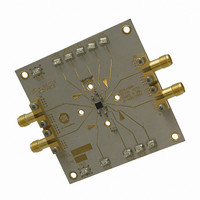
EVAL BOARD FOR NB4L16MMN
Manufacturer
ON Semiconductor
Datasheet
1.NB4L16MMNR2G.pdf
(12 pages)
Specifications of NB4L16MMNEVB
Main Purpose
Timing, Clock Buffer / Driver / Receiver / Translator
Embedded
No
Utilized Ic / Part
NB4L16M
Primary Attributes
Input Up To 5Gb/s & 3.5GHz
Secondary Attributes
Differential CML Output
Technology Type
Evaluation Board
Lead Free Status / RoHS Status
Lead free / RoHS Compliant
For Use With/related Products
NB4L16M
Other names
NB4L16MMNEVBOS


NOTE: Device will meet the specifications after thermal equilibrium has been established when mounted in a test socket or printed circuit
8. Measured by forcing V
9. Duty cycle skew is measured between differential outputs using the deviations of the sum of Tpw− and Tpw+ @ 0.5 GHz.
10. V
11. Additive RMS jitter with 50% duty cycle input clock signal.
12. Additive peak−to−peak data dependent jitter with NRZ input data signal, PRBS 2
13. Device−to−device skew is measured between outputs under identical transition @ 0.5 GHz.
Table 5. AC CHARACTERISTICS
Symbol
V
f
t
t
t
t
V
t
t
DATA
PLH
PHL
SKEW
JITTER
r
f
OUTPP
INPP
(20% − 80%). See Figure 12 and 14.
INPP
,
board with maintained transverse airflow greater than 500 lfpm. Electrical parameters are guaranteed only over the declared
operating temperature range. Functional operation of the device exceeding these conditions is not implied. Device specification limit
values are applied individually under normal operating conditions and not valid simultaneously.
(MAX) cannot exceed V
Output Voltage Amplitude (@V
(Figures 3 and 4)
Maximum Operating Data Rate
Propagation Delay to Output Differential @ 0.5 GHz
(Figure 6)
Duty Cycle Skew (Note 9)
Device−to−Device Skew (Note 13)
RMS Random Clock Jitter (Note 11)
Peak−to−Peak Data Dependent Jitter
(Note 12)
Input Voltage Swing/Sensitivity
(Differential Configuration) (Note 10)
Output Rise/Fall Times @ 0.5 GHz
(Figure 5)
INPP
(MIN) from a 50% duty cycle clock source. All loading with an external R
Characteristic
CC
− V
EE
V
. Input voltage swing is a single−ended measurement operating in differential mode. See Figure 11.
CC
INPPmin
= 2.375 V to 3.8 V, V
f
f
f
DATA
DATA
DATA
) f
(20% − 80%)
f
f
in
in
in
= 2.5 Gb/s
= 3.5 Gb/s
= 5.0 Gb/s
≤ 3.5 GHz
≤ 4.5 GHz
≤ 4.5 GHz
http://onsemi.com
EE
Min
280
150
175
3.5
75
= 0 V; (Note 8)
5
−40°C
Typ
400
300
215
5.0
2.0
6.0
0.2
1.5
2.0
9.0
60
−V
Max
V
23
265
0.7
10
90
10
12
25
90
CC
−1 and K28.7 pattern. See Figures 7, 8, 9, 10, 11 and 12.
EE
Min
280
150
175
3.5
75
25°C
Typ
400
300
220
5.0
2.0
6.0
0.2
1.5
2.0
9.0
60
L
= 50 W to V
−V
Max
V
265
0.7
10
90
10
12
25
90
CC
EE
Min
280
150
175
3.5
75
CC
. Input edge rates 40 ps
85°C
−V
V
Typ
400
300
225
5.0
2.0
6.0
0.2
1.5
2.0
9.0
60
CC
EE
Max
265
0.7
10
90
10
12
25
90
Gb/s
Unit
mV
mV
ps
ps
ps
ps
Related parts for NB4L16MMNEVB
Image
Part Number
Description
Manufacturer
Datasheet
Request
R

Part Number:
Description:
2.5v/3.3v, 5 Gb/s Multi Level Clock/data Input To Cml Driver / Receiver / Buffer / Translator With Internal Termination
Manufacturer:
ON Semiconductor
Datasheet:
Part Number:
Description:
ON Semiconductor [VOLTAGE REGULATOR]
Manufacturer:
ON Semiconductor
Datasheet:
Part Number:
Description:
357-036-542-201 CARDEDGE 36POS DL .156 BLK LOPRO
Manufacturer:
ON Semiconductor
Datasheet:
Part Number:
Description:
357-036-542-201 CARDEDGE 36POS DL .156 BLK LOPRO
Manufacturer:
ON Semiconductor
Datasheet:
Part Number:
Description:
357-036-542-201 CARDEDGE 36POS DL .156 BLK LOPRO
Manufacturer:
ON Semiconductor
Datasheet:
Part Number:
Description:
357-036-542-201 CARDEDGE 36POS DL .156 BLK LOPRO
Manufacturer:
ON Semiconductor
Datasheet:
Part Number:
Description:
357-036-542-201 CARDEDGE 36POS DL .156 BLK LOPRO
Manufacturer:
ON Semiconductor
Datasheet:
Part Number:
Description:
357-036-542-201 CARDEDGE 36POS DL .156 BLK LOPRO
Manufacturer:
ON Semiconductor
Datasheet:
Part Number:
Description:
357-036-542-201 CARDEDGE 36POS DL .156 BLK LOPRO
Manufacturer:
ON Semiconductor
Datasheet:
Part Number:
Description:
357-036-542-201 CARDEDGE 36POS DL .156 BLK LOPRO
Manufacturer:
ON Semiconductor
Datasheet:
Part Number:
Description:
357-036-542-201 CARDEDGE 36POS DL .156 BLK LOPRO
Manufacturer:
ON Semiconductor
Datasheet:
Part Number:
Description:
357-036-542-201 CARDEDGE 36POS DL .156 BLK LOPRO
Manufacturer:
ON Semiconductor
Datasheet:
Part Number:
Description:
Manufacturer:
ON Semiconductor
Datasheet:
Part Number:
Description:
Manufacturer:
ON Semiconductor
Datasheet: