NBC124XXEVB ON Semiconductor, NBC124XXEVB Datasheet
NBC124XXEVB
Specifications of NBC124XXEVB


Related parts for NBC124XXEVB

NBC124XXEVB Summary of contents
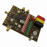
Page 1
NBC12430, NBC12430A 3.3V/5V Programmable PLL Synthesized Clock Generator 50 MHz to 800 MHz The NBC12430 and NBC12430A are general purpose, PLL based synthesized clock sources. The VCO will operate over a frequency range of 400 MHz to 800 MHz. The VCO ...
Page 2
MHz F with 16 MHz Crystal XTAL_SEL 2 FREF_EXT 9−BIT XTAL1 COUNTER 10−20MHz OSC 5 XTAL2 S_LOAD 7 P_LOAD 27 S_DATA 26 S_CLOCK Table 1. Output Division N [1:0] Output ...
Page 3
S_CLOCK S_DATA S_LOAD PLL_V CC FREF_EXT XTAL_SEL XTAL1 S_CLOCK 1 S_DATA 2 S_LOAD 3 PLL_V 4 CC PLL_V 5 CC FREF_EXT 6 XTAL_SEL 7 XTAL1 Figure 3. 32−Lead QFN ...
Page 4
The following gives a brief description of the functionality of the NBC12430 and NBC12430A Inputs and Outputs. Unless explicitly stated, all inputs are CMOS/TTL compatible with either pullup or pulldown resistors. The PECL outputs are capable of driving two series ...
Page 5
Table 4. ATTRIBUTES Internal Input Pulldown Resistor Internal Input Pullup Resistor ESD Protection Moisture Sensitivity (Note 1) Flammability Rating Transistor Count Meets or exceeds JEDEC Spec EIA/JESD78 IC Latchup Test 1. For additional information, see Application Note AND8003/D. Table 5. ...
Page 6
Table 6. DC CHARACTERISTICS (V Symbol V Input HIGH Voltage IH LVCMOS/ LVTTL V Input LOW Voltage IL LVCMOS/ LVTTL I Input Current IN V Output HIGH Voltage OH PECL V Output LOW Voltage OL PECL I Power Supply Current ...
Page 7
Table 8. AC CHARACTERISTICS (V (Note 7) Symbol Characteristic F Maximum Input Frequency MAXI F Maximum Output Frequency MAXO t Maximum PLL Lock Time LOCK t Period Jitter (RMS) jitter(pd) t Cycle−to−Cycle Jitter (Peak−to−Peak) jitter(cyc−cyc) t Setup Time s t ...
Page 8
The internal oscillator uses the external quartz crystal as the basis of its frequency reference. The output of the reference oscillator is divided by 16 before being sent to the phase detector. With a 16 MHz crystal, this provides a ...
Page 9
Programming the NBC12430 and NBC12430A is accomplished by properly configuring the internal dividers to produce the desired frequency at the outputs. The output frequency can by represented by this formula: F OUT + ((F XTAL or F REF_EXT ) B ...
Page 10
Table 11. Frequency Operating Range Á Á Á Á Á Á Á Á Á Á Á Á Á Á Á Á Á Á Á Á Á Á Á Á VCO Frequency (MHz) Range for a Crystal Frequency (MHz) of: Á ...
Page 11
Most of the signals available on the TEST output pin are useful only for performance verification of the device itself. However, the PLL bypass mode may be of interest at the board level for functional debug. When T[2:0] is set ...
Page 12
Using the On−Board Crystal Oscillator The NBC12430 and NBC12430A feature a fully integrated on−board crystal oscillator to minimize system implementation costs. The oscillator is a series resonant, multivibrator type design as opposed to the more common parallel resonant oscillator design. ...
Page 13
The parallel capacitor combination shown ensures that a low impedance path to ground exists for frequencies well above the bandwidth ...
Page 14
JITTER(cycle−cycle) 1 Figure 11. Cycle−to−Cycle Jitter Peak−to−Peak Jitter is the difference between the highest and lowest acquired value and is represented as the width of the Gaussian base. Time Figure 12. Peak−to−Peak Jitter ...
Page 15
S_DATA S_CLOCK t SETUP Figure 15. Setup and Hold S_DATA t S_LOAD SETUP Figure 16. Setup and Hold M[8:0] N[1:0] P_ LOAD t SETUP Figure 17. Setup and Hold F OUT F OUT Pulse Width Figure 18. Output Duty Cycle ...
Page 16
Driver Device Figure 19. Typical Termination for Output Driver and Device Evaluation (See Application Note AND8020 − Termination of ECL Logic Devices.) ORDERING INFORMATION Device NBC12430FA NBC12430FAG NBC12430FAR2 NBC12430FAR2G NBC12430FN NBC12430FNG NBC12430FNR2 NBC12430FNR2G NBC12430AFA NBC12430AFAG NBC12430AFAR2 NBC12430AFAR2G NBC12430AFN NBC12430AFNG NBC12430AFNR2 ...
Page 17
Resource Reference of Application Notes AN1405/D − ECL Clock Distribution Techniques AN1406/D − Designing with PECL (ECL at +5.0 V) AN1503/D − ECLinPSt I/O SPiCE Modeling Kit AN1504/D − Metastability and the ECLinPS Family AN1568/D − Interfacing Between LVDS and ...
Page 18
0.010 (0.250 NOTES: 1. DATUMS -L-, -M-, AND -N- DETERMINED WHERE TOP OF LEAD SHOULDER EXITS PLASTIC BODY AT ...
Page 19
−T− DETAIL −Z− −AB− −AC− SEATING PLANE 0.10 (0.004) AC NOTES: 1. DIMENSIONING AND TOLERANCING PER ANSI Y14.5M, 1982. 2. CONTROLLING DIMENSION: MILLIMETER. 3. DATUM PLANE ...
Page 20
... X 0.28 *For additional information on our Pb−Free strategy and soldering details, please download the ON Semiconductor Soldering and Mounting Techniques Reference Manual, SOLDERRM/D. N. American Technical Support: 800−282−9855 Toll Free USA/Canada Europe, Middle East and Africa Technical Support: Phone: 421 33 790 2910 Japan Customer Focus Center Phone: 81− ...