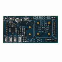
CDB2300-DC-LCO-CP Cirrus Logic Inc, CDB2300-DC-LCO-CP Datasheet - Page 9

CDB2300-DC-LCO-CP
Manufacturer Part Number
CDB2300-DC-LCO-CP
Description
BOARD EVAL GEN PURPOSE PLL
Manufacturer
Cirrus Logic Inc
Datasheet
1.CDB2000-PC-LCO.pdf
(26 pages)
Specifications of CDB2300-DC-LCO-CP
Main Purpose
Timing, Clock Generator
Embedded
No
Utilized Ic / Part
CS2000
Primary Attributes
Fractional-N, 6 ~ 75 MHz Low Jitter Clock Synthesizer, Clock Multiplier
Secondary Attributes
USB, I2C, SPI Interface
Product
Audio Modules
Lead Free Status / RoHS Status
Contains lead / RoHS non-compliant
Lead Free Status / RoHS Status
Lead free / RoHS Compliant, Contains lead / RoHS non-compliant
Other names
598-1494
CDB-2300-DC-LCO-CP
CDB-2300-DC-LCO-CP
DS821DB1
2.3.2
4. Launch the CS2000 Family Configuration Wizard.
5. Using the “CDK Controls” menu, select “Connect to CDK2000”.
6. Click “yes” to establish a connection with the board; Then press “OK” on the USBXpress success
7. If the device in the socket does not match the current GUI configuration you will get the “Warning!
8. Use the graphical user interface to define the device’s operation. Alternatively, choose “File -> Load
9. Evaluate the current configuration by toggling the state of the “Mode Select” drop down and by
10. Repeat steps 8-
11. Once the desired configuration is achieved select “CDK Controls -> Write Preview Data to MCU...”
Device Programming - Development Mode
12. To program the one-time-programmable memory in the CS2000 family device using the Wizard
13. To program the one-time-programmable memory in the CS2000 family device using the hardware
14. After the programming sequence is complete, the CS2000 family device will be able to operate in
15. To power-off the evaluation platform, ensure that the CDK2000 Configuration Wizard application is
message.
Device mismatch!” message. Click “Yes” to allow the GUI to configure itself according to the device
on the CDK2000. If this is not the device you intended to evaluate then click “No” which powers down
the device and you may then change the daughter card to the appropriate device.
Configuration” to load a pre-configured device configuration.
Note: The settings will not yet be programmed into the one-time-programmable memory. The Wizard
presents the user with a graphical controls over an internal virtual representation of the M2, M1, and
M0 pins. The purpose of these controls is to facilitate the evaluation of the device’s currently
previewed configuration. These graphical controls can be toggled, and the device will respond exactly
as it will once the configuration is programmed into one-time-programmable memory and the M2, M1,
and M0 pins are toggled.
pressing the M2 Low/High button, checking the device’s functionality for the desired response.
from the Wizard to save the current configuration to memory within the microcontroller on the
CDB2000-MB
This step downloads the current configuration into Flash memory within the microcontroller. Once this
step is complete, a one-time-programmable memory programming sequence can be initiated by
either software control through the Wizard or hardware control through a push-button on the
CDB2000-MB.
software, select “CDK Controls -> Initiate OTP Sequence...”.
controls on the CDB2000-MB
a) Close the Wizard software.
b) Verify that D9 is lit, indicating that the CS2000 family device is in hardware mode.
c) Place DIP switch position 5 into the upper (or opened) position to select Development mode.
d) Press and hold the on-board push-button (S1) for more than 1 second to program the OTP
memory.
hardware mode as defined by the programmed configuration. Simply ensure that the CDK2000
Configuration Wizard application is closed, and verify that D9 is lit indicating that the CS2000 family
device is in hardware mode. The M2, M1, and M0 switches on the CDB2000-MB will control its
operation.
closed and remove the USB cable from the CDB2000-MB.
The following steps reference the CDB2000-MB hardware.
9
until the desired configuration is achieved.
CDK2000
9


