AD5162EVAL Analog Devices Inc, AD5162EVAL Datasheet - Page 14
AD5162EVAL
Manufacturer Part Number
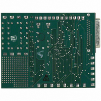
AD5162EVAL
Description
BOARD EVAL FOR AD5162
Manufacturer
Analog Devices Inc
Datasheet
1.AD5162BRMZ2.5.pdf
(20 pages)
Specifications of AD5162EVAL
Main Purpose
Digital Potentiometer
Utilized Ic / Part
AD5162
Lead Free Status / RoHS Status
Contains lead / RoHS non-compliant
Secondary Attributes
-
Embedded
-
Primary Attributes
-


AD5162
PROGRAMMING THE POTENTIOMETER DIVIDER
Voltage Output Operation
The digital potentiometer easily generates a voltage divider at
wiper to B and wiper to A, proportional to the input voltage at
A to B. Unlike the polarity of V
positive, voltage across A to B, W to A, and W to B can be at
either polarity.
If ignoring the effect of the wiper resistance for approximation,
connecting the A terminal to 5 V and the B terminal to ground
produces an output voltage at the wiper to B, starting at 0 V up
to 1 LSB less than 5 V. Each LSB of voltage is equal to the voltage
applied across the A and B terminals divided by the 256 positions
of the potentiometer divider. The general equation defining the
output voltage at V
voltage applied to Terminal A and Terminal B is
A more accurate calculation, which includes the effect of wiper
resistance, V
Operation of the digital potentiometer in the divider mode
results in more accurate operation over temperature. Unlike in
the rheostat mode, the output voltage is dependent mainly on
the ratio of the internal resistors R
values. Therefore, the temperature drift reduces to 15 ppm/°C.
V
V
W
W
(
(
D
D
)
)
=
W
=
Figure 35. Potentiometer Mode Configuration
, is
256
R
D
WB
R
AB
V
(
W
D
A
with respect to ground for any valid input
V
)
I
+
V
256
A
+
256
A
B
−
R
WA
D
R
DD
W
AB
WA
V
(
D
to GND, which must be
B
and R
)
V
V
B
O
WB
, not on the absolute
Rev. C | Page 14 of 20
(3)
(4)
ESD PROTECTION
All digital inputs are protected with a series of input resistors
and parallel Zener ESD structures, as shown in Figure 36 and
Figure 37. This applies to the SDI, CLK, and CS
TERMINAL VOLTAGE OPERATING RANGE
The AD5162 V
conditions for proper 3-terminal digital potentiometer opera-
tion. Supply signals present on the A, B, and W terminals that
exceed V
diodes (see Figure 38).
POWER-UP SEQUENCE
Because the ESD protection diodes limit the voltage compliance
at the A, B, and W terminals (see Figure 38), it is important to
power V
terminals; otherwise, the diode is forward-biased such that V
is powered unintentionally and may affect the rest of the user’s
circuit. The ideal power-up sequence is in the following order:
GND, V
order of powering V
important, as long as they are powered after V
Figure 38. Maximum Terminal Voltages Set by V
DD
DD
DD
, digital inputs, and then V
/GND before applying voltage to the A, B, and W
or GND are clamped by the internal forward-biased
Figure 37. ESD Protection of Resistor Terminals
DD
Figure 36. ESD Protection of Digital Pins
and GND power supply defines the boundary
A
, V
A, B, W
GND
GND
B
340Ω
, V
W
, and the digital inputs is not
LOGIC
A
, V
V
A
W
B
GND
B
DD
, V
W
digital input pins.
. The relative
DD
DD
/GND.
and GND
DD
Related parts for AD5162EVAL
Image
Part Number
Description
Manufacturer
Datasheet
Request
R


Part Number:
Description:
Board Mount Temperature Sensors TEMP MONITR DUAL CHN W/SERIES RSTNCE CNCL
Manufacturer:
ON Semiconductor
Datasheet:

Part Number:
Description:
Touch Screen Digitizer
Manufacturer:
Analog Devices, Inc.
Datasheet:
Part Number:
Description:
Half-duplex Icoupler-r Isolated Rs-485 Transceiver
Manufacturer:
Analog Devices, Inc.
Datasheet:

Part Number:
Description:
±1.7g Dual-Axis IMEMS Accelerometer Evaluation Board
Manufacturer:
Analog Devices Inc
Datasheet:

Part Number:
Description:
Inertial Sensor Evaluation System
Manufacturer:
Analog Devices Inc
Datasheet:
Part Number:
Description:
Manufacturer:
Analog Devices Inc
Datasheet:
Part Number:
Description:
Manufacturer:
Analog Devices Inc
Datasheet:
Part Number:
Description:
Manufacturer:
Analog Devices Inc
Datasheet:
Part Number:
Description:
Manufacturer:
Analog Devices Inc
Datasheet:
Part Number:
Description:
Manufacturer:
Analog Devices Inc
Datasheet: