CDB1600 Cirrus Logic Inc, CDB1600 Datasheet - Page 2
CDB1600
Manufacturer Part Number
CDB1600
Description
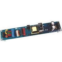
DEVELOPMENT BOARD FOR CS1600
Manufacturer
Cirrus Logic Inc
Specifications of CDB1600
Main Purpose
Power Management, Power Factor Correction
Embedded
No
Utilized Ic / Part
CS1600
Primary Attributes
460V, 1150W output
Secondary Attributes
108 ~ 305 VAC
Silicon Manufacturer
Cirrus Logic
Application Sub Type
Power Factor Correction (PFC)
Kit Application Type
Power Management
Silicon Core Number
CS1600
Lead Free Status / RoHS Status
Contains lead / RoHS non-compliant
Other names
598-1806
CDB1600
CDB1600


1. INTRODUCTION
The CS1600 digital power factor controller operates in variable
on-time, variable frequency, discontinuous conduction mode
(DCM). The CS1600 uses a proprietary digital algorithm to
maximize the efficiency and reduce the conductive EMI.
The analog-to-digital converter (ADC) shown in the CS1600
block diagram in Figure 9 is used to sense the PFC output
voltage ( V
measuring currents through their respective resistors. The
magnitudes of these currents are measured as a proportion of a
reference current (I
ADCs. The digital signal is then processed in a control algorithm
which determines the behavior of the CS1600 during start-up,
normal operation, and under fault conditions, such as
overvoltage, and over-temperature conditions.
The CS1600 PFC switching frequency varies with the V
a cycle-by-cycle basis, and its digital algorithm calculates the
on-time accordingly for unity power factor. Unlike traditional
Critical Conduction Mode (CRM) PFC controller, CS1600
operates at its low switching frequency near the zero-crossing
point of the AC input voltage, and it operates at its high
switching frequency at the peak of its AC input voltage (this is
the opposite of the switching frequency profile for a CRM PFC
controller), thus CS1600 reduces switching losses especially
under light-load conditions, spreads conducted EMI energy
peaks over a wide frequency band and increases overall
system efficiency.
The proprietary digital control engine optimizes the feedback
error signal using an adaptive control algorithm, improves
2
link
IAC
IFB
) and the rectified AC line voltage ( V
REF
3
4
) that functions as the reference for the
V
V
DD
DD
15k
15k
24k
24k
ADC
ADC
Figure 1. CS1600 Block Diagram
rect
rect
) by
on
Regulator
Voltage
system stability and transient response. No external feedback
error signal compensation components are required.
The CS1600s digital controller algorithm limits the ON time of
the Power MOSFET by the following equation:
Where T
on and V
sudden line surge or sporadic, high dv/dt line voltages, this
equation may not limit the ON time appropriately. For this type
of line disturbance, additional protection mechanisms such as
fusible resistors, fast-blow fuses, or other current-limiting
devices are recommended.
Under steady-state conditions, the voltage loop keeps PFC
output voltage close to its nominal value. Under light load
startup or feedback loop open conditions, the output voltage
may pass the overvoltage protection threshold. The digital
control engine initiates a fast response loop to shut down gate
driving signal to reduce the energy delivered to the output for
PFC capacitor protection. When the link voltage drop below
V
OVP
POR
– V
+
-
on
OVP(Hy)
rect
V
V
is the max time that the power MOSFET is turned
th(ST)
th(STP)
is the rectified line voltage. In the event of a
, PFC resumes normal operation.
V
T
Z
on
V
0.001827V S
------------------------------------ -
DD
V
rect
6
5
7
VDD
GD
GND
CS1600
DS904F1
Related parts for CDB1600
Image
Part Number
Description
Manufacturer
Datasheet
Request
R

Part Number:
Description:
Development Kit
Manufacturer:
Cirrus Logic Inc
Datasheet:
Part Number:
Description:
Development Kit
Manufacturer:
Cirrus Logic Inc
Datasheet:


Part Number:
Description:
High-efficiency PFC + Fluorescent Lamp Driver Reference Design
Manufacturer:
Cirrus Logic Inc
Datasheet:
Part Number:
Description:
Development Kit
Manufacturer:
Cirrus Logic Inc
Datasheet:
Part Number:
Description:
Development Kit
Manufacturer:
Cirrus Logic Inc
Datasheet:

Part Number:
Description:
Development Kit
Manufacturer:
Cirrus Logic Inc
Datasheet:
Part Number:
Description:
Development Kit
Manufacturer:
Cirrus Logic Inc
Datasheet:
Part Number:
Description:
Development Kit
Manufacturer:
Cirrus Logic Inc
Datasheet:
Part Number:
Description:
Development Kit
Manufacturer:
Cirrus Logic Inc
Datasheet:

Part Number:
Description:
EVALUATION BOARD FOR CS8427
Manufacturer:
Cirrus Logic Inc
Datasheet:

Part Number:
Description:
BOARD EVAL FOR CS8416 RCVR
Manufacturer:
Cirrus Logic Inc
Datasheet:

Part Number:
Description:
EVALUATION BOARD FOR CS8420
Manufacturer:
Cirrus Logic Inc
Datasheet:

Part Number:
Description:
KIT DEVELOPMENT EP9315 ARM9
Manufacturer:
Cirrus Logic Inc
Datasheet:

Part Number:
Description:
KIT DEVELOPMENT EP9302 ARM9
Manufacturer:
Cirrus Logic Inc
Datasheet: