EVAL-ADF4118EB1 Analog Devices Inc, EVAL-ADF4118EB1 Datasheet - Page 2
EVAL-ADF4118EB1
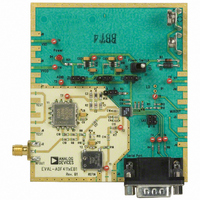
Manufacturer Part Number
EVAL-ADF4118EB1
Description
BOARD EVAL FOR ADF4118
Manufacturer
Analog Devices Inc
Datasheet
1.ADF4116BRUZ-REEL.pdf
(28 pages)
Specifications of EVAL-ADF4118EB1
Main Purpose
Timing, Frequency Synthesizer
Embedded
No
Utilized Ic / Part
ADF4118
Primary Attributes
Single Integer-N PLL
Secondary Attributes
1.96GHz WCDMA, Graphical User Interface
Lead Free Status / RoHS Status
Contains lead / RoHS non-compliant


ADF4116/ADF4117/ADF4118
TABLE OF CONTENTS
Features .............................................................................................. 1
Applications....................................................................................... 1
General Description ......................................................................... 1
Functional Block Diagram .............................................................. 1
Revision History ............................................................................... 2
Specifications..................................................................................... 3
Absolute Maximum Ratings............................................................ 6
Pin Configuration and Function Descriptions............................. 7
Typical Performance Characteristics ............................................. 8
Circuit Description......................................................................... 12
REVISION HISTORY
4/07—Rev. C to Rev. D
Changes to REF
Changes to Table 4............................................................................ 7
Changes to Figure 35...................................................................... 22
Changes to Ordering Guide .......................................................... 25
11/05—Rev. B to Rev. C
Changes to Table 1............................................................................ 3
Changes to Table 2............................................................................ 5
Changes to Table 3............................................................................ 6
Changes to Table 4............................................................................ 7
Changed OSC 3B1-13M0 to FOX801BH-130 ............................ 21
Changes to Ordering Guide .......................................................... 25
Timing Characteristics ................................................................ 5
ESD Caution.................................................................................. 6
Reference Input Section............................................................. 12
RF Input Stage............................................................................. 12
Prescaler (P/P + 1)...................................................................... 12
A Counter and B Counter ......................................................... 12
R Counter .................................................................................... 12
Phase Frequency Detector (PFD) and Charge Pump............ 13
MUXOUT and Lock Detect...................................................... 13
Input Shift Register..................................................................... 13
IN
Characteristics Section..................................... 3
Rev. D | Page 2 of 28
Function Latch................................................................................ 19
Applications Information .............................................................. 21
Outline Dimensions ....................................................................... 25
9/04—Rev. A to Rev. B
Changes to Specifications.................................................................3
Changes to Ordering Guide .......................................................... 25
3/01—Rev. 0 to Rev. A
4/00—Rev. 0: Initial Version
Latch Summaries ........................................................................ 14
Latch Maps .................................................................................. 15
Counter Reset ............................................................................. 19
Power-Down ............................................................................... 19
MUXOUT Control..................................................................... 19
Phase Detector Polarity ............................................................. 19
Charge Pump Three-State......................................................... 19
Fastlock Enable Bit ..................................................................... 19
Fastlock Mode Bit....................................................................... 19
Timer Counter Control ............................................................. 19
Initialization Latch ..................................................................... 20
Device Programming After Initial Power-Up ........................ 20
Local Oscillator for the GSM Base Station Transmitter........ 21
Shutdown Circuit ....................................................................... 21
Direct Conversion Modulator .................................................. 21
Interfacing ................................................................................... 24
Ordering Guide .......................................................................... 25
Related parts for EVAL-ADF4118EB1
Image
Part Number
Description
Manufacturer
Datasheet
Request
R


Part Number:
Description:
BOARD EVAL FOR SI270X-A
Manufacturer:
Silicon Laboratories Inc
Datasheet:

Part Number:
Description:
BUCK CONV REF DESIGN KIT IP1201
Manufacturer:
International Rectifier
Datasheet:
Part Number:
Description:
BOARD DEMO SYNC DUAL BUCK CNVTER
Manufacturer:
International Rectifier
Datasheet:
Part Number:
Description:
BOARD DEMO SYNC BUCK CONVETER
Manufacturer:
International Rectifier
Datasheet:

Part Number:
Description:
EVALBOARD/EB Omnidirectional microphone - Analog
Manufacturer:
Analog Devices
Datasheet:
Part Number:
Description:
EVALBOARD/EB Omnidirectional microphone - Analog
Manufacturer:
Analog Devices
Datasheet:


Part Number:
Description:
BOARD EVAL LED DRIVER LT3756
Manufacturer:
Linear Technology
Datasheet:

Part Number:
Description:
BOARD EVAL FOR AD7741/7742
Manufacturer:
Analog Devices Inc
Datasheet:

Part Number:
Description:
±1.7g Dual-Axis IMEMS Accelerometer Evaluation Board
Manufacturer:
Analog Devices Inc
Datasheet:

Part Number:
Description:
IC MULTIPLIER ANALOG 8-SOIC T/R
Manufacturer:
Analog Devices Inc
Datasheet:

Part Number:
Description:
IC ANALOG MULTIPLIER 8-DIP
Manufacturer:
Analog Devices Inc
Datasheet:
Part Number:
Description:
IC ANALOG MULTIPLIER 8-SOIC
Manufacturer:
Analog Devices Inc
Datasheet:
Part Number:
Description:
IC ANALOG MULTIPLIER 8-DIP
Manufacturer:
Analog Devices Inc
Datasheet: