AD9520-4/PCBZ Analog Devices Inc, AD9520-4/PCBZ Datasheet - Page 37
AD9520-4/PCBZ
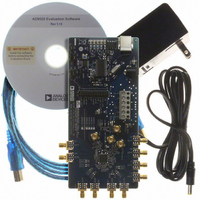
Manufacturer Part Number
AD9520-4/PCBZ
Description
BOARD EVAL FOR AD9520-4
Manufacturer
Analog Devices Inc
Specifications of AD9520-4/PCBZ
Design Resources
Synchronizing Multiple AD9910 1 GSPS Direct Digital Synthesizers (CN0121) Phase Coherent FSK Modulator (CN0186)
Main Purpose
Timing, Clock Generator
Embedded
No
Utilized Ic / Part
AD9520-4
Primary Attributes
1.4 ~ 1.8 GHz Output Frequency
Secondary Attributes
Accepts CMOS, LVDS, or LVPECL References Up to 250 MHz
Silicon Manufacturer
Analog Devices
Application Sub Type
PLL Clock Synthesizer
Kit Application Type
Clock & Timing
Silicon Core Number
AD9520-0, AD9520-2, AD9520-2
Silicon Family Name
AD9520-X
Rohs Compliant
Yes
Lead Free Status / RoHS Status
Lead free / RoHS Compliant


Prescaler
The prescaler of the AD9520 allows for two modes of operation:
a fixed divide (FD) mode of 1, 2, or 3 and a dual modulus (DM)
mode where the prescaler divides by P and (P + 1) {2 and 3, 4
and 5, 8 and 9, 16 and 17, or 32 and 33}. The prescaler modes of
operation are given in Table 53, 0x016[2:0]. Not all modes are
available at all frequencies (see Table 2).
When operating the AD9520 in dual modulus mode, P/(P + 1),
the equation used to relate the input reference frequency to the
VCO output frequency is
However, when operating the prescaler in FD mode 1, 2, or 3,
the A counter is not used (A = 0) and the equation simplifies to
When A = 0, the divide is a fixed divide of P = 2, 4, 8, 16, or 32.
By using combinations of DM and FD modes, the AD9520 can
achieve values of N all the way down to N = 1. Table 29 shows
how a 10 MHz reference input can be locked to any integer
multiple of N.
Note that the same value of N can be derived in different ways,
as illustrated by the case of N = 12. The user can choose a fixed
divide mode P = 2 with B = 6, use the dual modulus mode 2/3
with A = 0, B = 6, or use the dual modulus mode 4/5 with
A = 0, B = 3.
Table 29. How a 10 MHz Reference Input Can Be Locked to Any Integer Multiple of N
f
10
10
10
10
10
10
10
10
10
10
10
10
10
10
10
10
10
1
REF
X = don’t care.
(MHz)
f
f
VCO
VCO
= (f
= (f
REF
REF
R
1
1
1
1
1
1
1
1
1
1
1
1
1
1
1
1
1
/R) × (P × B + A) = f
/R) × (P × B) = f
P
1
2
1
1
1
2
2
2
2
2
2
2
2
2
2
4
4
A
X
X
X
X
X
X
0
1
2
1
X
0
1
X
0
0
1
1
1
1
1
1
1
1
1
REF
× N/R
B
1
1
3
4
5
3
3
3
3
4
5
5
5
6
6
3
3
REF
× N/R
N
1
2
3
4
5
6
6
7
8
9
10
10
11
12
12
12
13
f
10
20
30
40
50
60
60
70
80
90
100
100
110
120
120
120
130
VCO
(MHz)
Rev. 0 | Page 37 of 84
Mode
FD
FD
FD
FD
FD
FD
DM
DM
DM
DM
FD
DM
DM
FD
DM
DM
DM
A and B Counters
The AD9520 B counter can be bypassed (B = 1). This B counter
bypass mode is only valid when using the prescaler in FD mode.
When A = 0, the divide is a fixed divide of P = 2, 4, 8, 16, or 32.
Unlike the R counter, an A = 0 is actually zero. The B counter
must be ≥3 or bypassed.
The maximum input frequency to the A/B counter is reflected
in the maximum prescaler output frequency (~300 MHz) specified
in Table 2. This is the prescaler input frequency (VCO or CLK)
divided by P.
Although manual reset is not normally required, the A/B counters
have their own reset bit. The A and B counters can be reset using
the shared reset bit of the R, A, and B counters. They can also
be reset through a SYNC operation.
R, A, and B Counters: SYNC Pin Reset
The R, A, and B counters can also be reset simultaneously
through the SYNC pin. This function is controlled by 0x019[7:6]
(see
R and N Divider Delays
Both the R and N dividers feature a programmable delay cell.
These delays can be enabled to allow adjustment of the phase
relationship between the PLL reference clock and the VCO or
CLK. Each delay is controlled by three bits. The total delay
range is about 1 ns. See 0x019 in Table 53.
Table 53
Notes
P = 1, B = 1 (bypassed)
P = 2, B = 1 (bypassed)
P = 1, B = 3
P = 1, B = 4
P = 1, B = 5
P = 2, B = 3
P and P + 1 = 2 and 3, A = 0, B = 3
P and P + 1 = 2 and 3, A = 1, B = 3
P and P + 1 = 2 and 3, A = 2, B = 3
P and P + 1 = 2 and 3, A = 1, B = 4
P = 2, B = 5
P and P + 1 = 2 and 3, A = 0, B = 5
P and P + 1 = 2 and 3, A = 1, B = 5
P = 2, B = 6
P and P + 1 = 2 and 3, A = 0, B = 6
P and P + 1 = 4 and 5, A = 0, B = 3
P and P + 1 = 4 and 5, A = 1, B = 3
). The
SYNC pin reset is disabled by default.
AD9520-4
Related parts for AD9520-4/PCBZ
Image
Part Number
Description
Manufacturer
Datasheet
Request
R

Part Number:
Description:
12/24 Channel Clock Gen 2,0GH
Manufacturer:
Analog Devices Inc
Datasheet:

Part Number:
Description:
12/24 Channel Clock Gen 2,0GH
Manufacturer:
Analog Devices Inc
Datasheet:
Part Number:
Description:
12/24 Channel Clock Gen 2,0GH
Manufacturer:
Analog Devices Inc
Datasheet:
Part Number:
Description:
12/24 Channel Clock Gen 2,0GH
Manufacturer:
Analog Devices Inc
Datasheet:
Part Number:
Description:
12/24 Channel Clock Gen 2,0GH
Manufacturer:
Analog Devices Inc
Datasheet:
Part Number:
Description:
Clock IC With 2.8GHz On-chip VCO
Manufacturer:
Analog Devices Inc
Datasheet:
Part Number:
Description:
Lock IC With 2.8GHz On-chip VCO
Manufacturer:
Analog Devices Inc
Datasheet:
Part Number:
Description:
12/24 Channel Clock Gen 2,5 GHz VCO
Manufacturer:
Analog Devices Inc
Datasheet:
Part Number:
Description:
12/24 Channel Clock Distribution W/ On-C
Manufacturer:
Analog Devices Inc
Datasheet:
Part Number:
Description:
12/24 Channel Clock Gen 2,25GH
Manufacturer:
Analog Devices Inc
Datasheet:
Part Number:
Description:
12/24 Channel Clock Distribution W/ On-C
Manufacturer:
Analog Devices Inc
Datasheet:
Part Number:
Description:
12/24 Channel Clock Distribution W/ On-C
Manufacturer:
Analog Devices Inc
Datasheet:
Part Number:
Description:
Clock IC With 1.6GHz On-chip VCO
Manufacturer:
Analog Devices Inc
Datasheet:
Part Number:
Description:
Clock IC With 1.6GHz On-chip VCO
Manufacturer:
Analog Devices Inc
Datasheet:
Part Number:
Description:
12/24-Output Clock Generator
Manufacturer:
Analog Devices Inc
Datasheet: