AD9551/PCBZ Analog Devices Inc, AD9551/PCBZ Datasheet - Page 18
AD9551/PCBZ
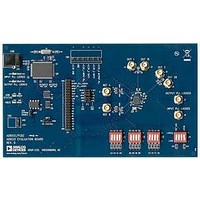
Manufacturer Part Number
AD9551/PCBZ
Description
BOARD EVAL FOR AD9951
Manufacturer
Analog Devices Inc
Datasheet
1.AD9551PCBZ.pdf
(40 pages)
Specifications of AD9551/PCBZ
Main Purpose
Timing, Clock Generator
Embedded
No
Utilized Ic / Part
AD9551
Primary Attributes
2 Inputs, 2 Outputs, VCO
Secondary Attributes
Graphical User Interface, USB Interface
Silicon Manufacturer
Analog Devices
Application Sub Type
Clock Generator
Kit Application Type
Clock & Timing
Silicon Core Number
AD9551
Kit Contents
Board
Lead Free Status / RoHS Status
Lead free / RoHS Compliant


AD9551
The reference DLL measures the period of the active reference
and produces the required N/2 delay value. When the reference
DLL locks, the following three events occur:
•
•
•
This implies that the signal driving the input PLL is the active
reference (after division by its input divider) with a half-cycle delay.
Because the alternate DLL is in closed-loop mode, and assuming
that the alternate reference is available, the output of the alternate
DLL is edge-aligned with the delayed output of the active DLL.
Furthermore, the closed-loop operation of the alternate DLL
causes its delay value to be adjusted dynamically so that it main-
tains nominal edge alignment with the output of the active DLL.
Edge alignment of the active and alternate references is the key
to the hitless switchover capability of the AD9551.
Reference Switchover and Holdover Mode
If the reference monitor detects the loss of the active reference,
it initiates the following three simultaneous operations:
•
•
•
Because the failed alternate reference is assigned to the alternate
DLL, upon its return the alternate DLL (which is in closed-loop
mode) automatically edge-aligns the delayed alternate reference
with the delayed active reference. Thus, if the new active reference
fails, switchover to the alternate reference occurs in a hitless
manner. This method of swapping the functionality of DLL A
and DLL B as either active (open-loop) or alternate (closed-loop)
allows for continuous hitless switching from one reference to
the other, as needed (assuming the availability of an alternate
reference upon failure of the active reference).
Note that if both references fail, the device enters holdover
mode. In this case, the reference monitor holds the DCXO at its
last setting prior to the holdover condition, and the DCXO free
runs at this setting until the holdover condition expires.
Forcing Selection of the Active Reference
Because the synchronization mechanism autonomously switches
between references, the user has no way of knowing which
reference is currently the active reference. However, the device
can be forced to select a specific input reference as the active
reference. For example, to force REFA to be the active reference,
power down the REFB input receiver by programming the appro-
priate registers (or disconnect the REFB signal source).
Both DLL A and DLL B are enabled.
The DLL associated with the active reference enters open-
loop mode.
The DLL associated with the alternate reference enters
closed-loop mode.
The output mux selects the output of the alternate DLL.
The alternate DLL holds its most recent delay setting (that
is, the delay setting that edge-aligned the output of the alter-
nate DLL with the output of the active DLL). Note that this
operation ensures hitless switching between references.
The new active reference is connected to the reference DLL
to measure its period (that is, a new N/2 value).
Rev. B | Page 18 of 40
The absence of a REFB signal causes the device to perform
a hitless switchover to REFA. If REFA is already the active
reference, the absence of REFB results in no action, and REFA
remains the active reference. In this way, the user can ensure
that REFA is the active reference. Likewise, by using the same
procedure but reversing the roles of the two references, the user
can force the device to select REFB as the active reference.
Digitally Controlled Crystal Oscillator (DCXO)
The DCXO is the fundamental building block of the input PLL
(see the Input PLL section). The DCXO relies on an external
crystal (19.44 MHz to 52 MHz) as its frequency source. The
resonant frequency of the external crystal varies as a function
of the applied load capacitance. The AD9551 has two internal
capacitor banks (static and dynamic) that provide the required
load capacitance. In operation, the control loop of the input PLL
automatically adjusts the value of the capacitive load to push or
pull the crystal resonant frequency over a small range of approxi-
mately ±50 ppm.
The tuning capacitor bank sets the static load capacitance, which
defaults to ~2 pF. The varactor bank is a dynamic capacitance
controlled by the DCXO to push or pull the crystal resonant
frequency. The nominal varactor capacitance is ~6 pF, and
when combined with the 2 pF static capacitance and 2 pF of
typical parasitic capacitance, the total crystal load capacitance is
~10 pF (default).
The user can alter the default load capacitance by changing
the static load capacitance of the tuning capacitor bank via
Register 0x1B[5:0]. These six bits set the static load capacitance
in 0.25 pF increments up to a maximum of ~16 pF.
The control loop of the input PLL locks the DCXO to the active
reference signal by dynamically controlling the varactor capaci-
tance. Note that the narrow frequency control range (±50 ppm) of
the varactor bank, combined with the default operating parameters
of the AD9551, dictate the use of a crystal with specified load
capacitance of 10 pF and a frequency tolerance of 20 ppm (see
the NDK NX3225SA, for example).
The narrow tuning range of the DCXO has two implications.
First, the user must properly choose the divide ratio of the input
reference divider to establish a frequency that is within the DCXO
tuning range. Second, the user must ensure that the jitter/wander
of the input reference is low enough to ensure the stability of the
input PLL control loop for applications where the DCXO is the
reference source for the output PLL (the default configuration).
Normally, the input SDMs help to mitigate the input jitter because
of the way they interact with the behavior of the input PLL. Input
jitter becomes an issue, however, when the input dividers operate
in integer-only mode or the input PLL is bypassed.
Related parts for AD9551/PCBZ
Image
Part Number
Description
Manufacturer
Datasheet
Request
R


Part Number:
Description:
±1.7g Dual-Axis IMEMS Accelerometer Evaluation Board
Manufacturer:
Analog Devices Inc
Datasheet:

Part Number:
Description:
Inertial Sensor Evaluation System
Manufacturer:
Analog Devices Inc
Datasheet:
Part Number:
Description:
Manufacturer:
Analog Devices Inc
Datasheet:
Part Number:
Description:
Manufacturer:
Analog Devices Inc
Datasheet:
Part Number:
Description:
Manufacturer:
Analog Devices Inc
Datasheet:
Part Number:
Description:
Manufacturer:
Analog Devices Inc
Datasheet:
Part Number:
Description:
Manufacturer:
Analog Devices Inc
Datasheet:
Part Number:
Description:
Manufacturer:
Analog Devices Inc
Datasheet:
Part Number:
Description:
Manufacturer:
Analog Devices Inc
Datasheet:
Part Number:
Description:
Manufacturer:
Analog Devices Inc
Datasheet:
Part Number:
Description:
Manufacturer:
Analog Devices Inc
Datasheet:
Part Number:
Description:
Manufacturer:
Analog Devices Inc
Datasheet: