CDB4270 Cirrus Logic Inc, CDB4270 Datasheet - Page 9
CDB4270
Manufacturer Part Number
CDB4270
Description
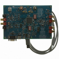
BOARD EVAL FOR CS4270 CODEC
Manufacturer
Cirrus Logic Inc
Datasheet
1.CDB4270.pdf
(50 pages)
Specifications of CDB4270
Main Purpose
Audio, CODEC
Embedded
Yes, FPGA / CPLD
Utilized Ic / Part
CS4270
Primary Attributes
Stereo, 24-Bit, 192 kHz Sample Rate
Secondary Attributes
I²S, S/PDIF Inputs and Outputs, Analog Inputs and Outputs, GUI
Description/function
Audio CODECs
Operating Supply Voltage
5 V
Product
Audio Modules
For Use With/related Products
CS4270
Lead Free Status / RoHS Status
Contains lead / RoHS non-compliant
Lead Free Status / RoHS Status
Lead free / RoHS Compliant, Contains lead / RoHS non-compliant
Other names
598-1002


DS686DB3
2. FPGA OVERVIEW
The FPGA (U11) controls all digital signal routing between the CS4270, CS8406, CS8416 and the DSP I/O Header.
The device also generates all of the clock/data driver output enables and S/PDIF device mode controls. The FPGA
internal registers can be configured either via the I²C (Software Mode) or via external dip switches (Hardware Mode).
When using the CS4270 in Hardware Mode, the FPGA decodes some of these dip-switch settings and generates
the CS4270 control signals. In addition, the FPGA distributes resets from the micro for all of the devices on the
board.
2.1
2.2
.
FPGA Architecture
Figures 3
the FPGA and the other devices on the board. The FPGA has an I²C interface and internal registers for soft-
ware control and can also read external dip-switch settings for hardware control. Refer to the
Register Description
Internal Sub-Clock Routing
Figure 3
CS8406 and DSP Header. Refer to the
description of the sub-clock routing register settings.
shows the internal sub-clock (SCLK, LRCK) routing topology between the CS4270, CS8416,
DSP Header
through
CS8416
LRCK
LRCK
SCLK
SCLK
5
SUBCLK.FROM.HDR
SUBCLK.FROM.HDR
show the internal architecture of the FPGA.
section of this document for a description of the FPGA registers.
SUBCLK.TO.HDR
SUBCLK.TO.HDR
Figure 3. Internal Sub-Clock Routing
CS8416-FPGA-LRCK
FPGA-CS8406-LRCK
CS8416-FPGA-LRCK
FPGA-DUT-LRCK
HDR-LRCK
HDR-LRCK
FPGA
FPGA-CS8406- LRCK
FPGA- DUT-LRCK
SUB_CK[1:0]
SUB_CK[1:0]
CS8416-FPGA-SCLK
HDR-SCLK
FPGA GUI Register Description
SUB_CK[1:0]
CS8416-FPGA-SCLK
FPGA-DUT-SCLK
FPGA-CS8406-SCLK
SUB_CK[1:0]
FPGA-DUT-SCLK
HDR-SCLK
FPGA-CS8406-SCLK
CS8416-FPGA-SCLK
FPGA-CS8406-SCLK
CS8416-FPGA-SCLK
FPGA-DUT-SCLK
FPGA-CS8406-SCLK
HDR-SCLK
HDR-SCLK
FPGA-DUT-SCLK
SUB_CK[1:0]
SUB_CK[1:0]
CS8416-FPGA- LRCK
HDR-LRCK
SUB_CK[1:0]
SUB_CK[1:0]
FPGA-DUT-LRCK
HDR-LRCK
FPGA-DUT-LRCK
FPGA-CS8406-LRCK
CS8416-FPGA-LRCK
FPGA-CS8406-LRCK
Figure 6
shows the MCLK routing to/from
section of this document for a
LRCK
SCLK
LRCK
SCLK
CS8406
CS4270
CDB4270
FPGA GUI
9
Related parts for CDB4270
Image
Part Number
Description
Manufacturer
Datasheet
Request
R

Part Number:
Description:
Development Kit
Manufacturer:
Cirrus Logic Inc
Datasheet:
Part Number:
Description:
Development Kit
Manufacturer:
Cirrus Logic Inc
Datasheet:


Part Number:
Description:
High-efficiency PFC + Fluorescent Lamp Driver Reference Design
Manufacturer:
Cirrus Logic Inc
Datasheet:
Part Number:
Description:
Development Kit
Manufacturer:
Cirrus Logic Inc
Datasheet:
Part Number:
Description:
Development Kit
Manufacturer:
Cirrus Logic Inc
Datasheet:

Part Number:
Description:
Development Kit
Manufacturer:
Cirrus Logic Inc
Datasheet:
Part Number:
Description:
Development Kit
Manufacturer:
Cirrus Logic Inc
Datasheet:
Part Number:
Description:
Development Kit
Manufacturer:
Cirrus Logic Inc
Datasheet:
Part Number:
Description:
Development Kit
Manufacturer:
Cirrus Logic Inc
Datasheet:

Part Number:
Description:
EVALUATION BOARD FOR CS8427
Manufacturer:
Cirrus Logic Inc
Datasheet:

Part Number:
Description:
BOARD EVAL FOR CS8416 RCVR
Manufacturer:
Cirrus Logic Inc
Datasheet:

Part Number:
Description:
EVALUATION BOARD FOR CS8420
Manufacturer:
Cirrus Logic Inc
Datasheet:

Part Number:
Description:
KIT DEVELOPMENT EP9315 ARM9
Manufacturer:
Cirrus Logic Inc
Datasheet:

Part Number:
Description:
KIT DEVELOPMENT EP9302 ARM9
Manufacturer:
Cirrus Logic Inc
Datasheet: