CY3272 Cypress Semiconductor Corp, CY3272 Datasheet - Page 15
CY3272
Manufacturer Part Number
CY3272
Description
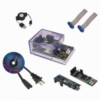
KIT EVAL POWERLINE HIGH VOLT
Manufacturer
Cypress Semiconductor Corp
Datasheet
1.CY3272.pdf
(34 pages)
Specifications of CY3272
Main Purpose
Interface, Transceiver, Powerline Communication
Embedded
No
Utilized Ic / Part
CY8CPLC10
Primary Attributes
2400bps Data Transfer Over High Voltage Power Lines
Secondary Attributes
LED Status Indicators
Silicon Manufacturer
Cypress
Silicon Core Number
CY8CPLC10
Kit Application Type
Communication & Networking
Application Sub Type
High Voltage Powerline Communication
Rohs Compliant
Yes
Lead Free Status / RoHS Status
Lead free / RoHS Compliant
Lead Free Status / RoHS Status
Lead free / RoHS Compliant, Lead free / RoHS Compliant
Other names
428-3008


2.3.4
CY3272 Cypress High Voltage Powerline Communication Evaluation Kit Guide, Doc. # 001-55381 Rev. *C
Figure 2-4. Coupling Circuit
Cypress Powerline Communication Transceiver and User Controls
This section has the CY8CPLC10 chip, which has the integrated transmit and receive modem, and
network protocol layer. It also has the I2C header to communicate with the external host processor.
The DIP switches to control the addresses and the jumpers to control the functionality of the chip are
also located in this section of the board. The red, blue, yellow, and green LEDs indicate the different
status of the board while functioning.
The key components and their detailed use are as follows:
Table 2-4. Transceiver and User Controls
The key components are circled in the following schematic.
CY8CPLC10
PWR LED[DS5]
TX LED[DS3]
RX LED[DS2]
BIU LED[DS4]
S1[3-5]
S1[2]
S1[1]
S2
Component
This is the Cypress powerline transceiver device. It is a 28 pin SSOP device.
This is a blue LED that glows when the board is powered on.
This is a green LED that glows when the board is transmitting data on to the powerline.
This is a red LED that glows when the CY8CPLC10 device is receiving data.
This is a yellow LED that glows when the transmit frequency band is in use.
These dip switches set up the logical address of the node in the network. These
switches provide an easy way to quickly assign an address from 0 to 7 to the board in a
network. S1[3] is MSB and S1[5] is LSB for logical address assignment. If the address is
modified, the board must be reset to reflect the changes.
This dip switch sets the I2C slave address to establish the communication with a host
processor. Setting the switch to OFF or ON will set the I2C address to external 0x01 or
0x7a respectively.
This dip switch controls the clock setting to the CY8CPLC10. Setting the switch to OFF
or ON will set the FSK modem clock to external 32 kHz crystal or external 24 MHz oscil-
lator, respectively. Note that the external crystal is always required for protocol timing.
Reset switch to reset the CY8CPLC10 chip.
Description/Comment
PLC HV Evaluation Board
15
[+] Feedback
Related parts for CY3272
Image
Part Number
Description
Manufacturer
Datasheet
Request
R

Part Number:
Description:
Manufacturer:
Cypress Semiconductor Corp
Datasheet:
Part Number:
Description:
Manufacturer:
Cypress Semiconductor Corp
Datasheet:
Part Number:
Description:
Manufacturer:
Cypress Semiconductor Corp
Datasheet:
Part Number:
Description:
Manufacturer:
Cypress Semiconductor Corp
Datasheet:
Part Number:
Description:
Manufacturer:
Cypress Semiconductor Corp
Datasheet: