LMX25120967EVAL/NOPB National Semiconductor, LMX25120967EVAL/NOPB Datasheet - Page 9
LMX25120967EVAL/NOPB
Manufacturer Part Number
LMX25120967EVAL/NOPB
Description
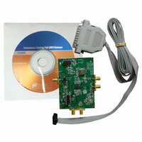
EVALUATION BOARD FOR LMX25120967
Manufacturer
National Semiconductor
Series
PLLatinum™r
Datasheets
1.LMX2512LQ0967NOPB.pdf
(18 pages)
2.LMX2430EVAL.pdf
(8 pages)
3.LMX25120967EVALNOPB.pdf
(24 pages)
Specifications of LMX25120967EVAL/NOPB
Main Purpose
Timing, Frequency Synthesizer
Embedded
No
Utilized Ic / Part
LMX2512
Primary Attributes
Single Fractional-N and Integer-N PLL with VCO
Secondary Attributes
967MHz, CodeLoader Graphical User Interface
Lead Free Status / RoHS Status
Lead free / RoHS Compliant
Other names
*LMX25120967EVAL
*LMX25120967EVAL/NOPB
LMX25120967EVAL
*LMX25120967EVAL/NOPB
LMX25120967EVAL


Functional Description
MICROWIRE INTERFACE
The programmable register set is accessed via the
MICROWIRE serial interface. The interface comprises three
signal pins: CLK, DATA, and LE (Latch Enable). Serial data
(DATA) is clocked into the 24-bit shift register on the rising
(Continued)
FIGURE 2. Lock Detect Flow Diagram
9
edge of the clock (CLK). The last bits decode the internal
control register address. When the latch enable (LE) transi-
tions from LOW to HIGH, data stored in the shift registers is
loaded into the corresponding control register.
20068006
www.national.com
Related parts for LMX25120967EVAL/NOPB
Image
Part Number
Description
Manufacturer
Datasheet
Request
R

Part Number:
Description:
National Semiconductor [8-Bit D/A Converter]
Manufacturer:
National Semiconductor
Datasheet:
Part Number:
Description:
National Semiconductor [Media Coprocessor]
Manufacturer:
National Semiconductor
Datasheet:
Part Number:
Description:
Digitally Controlled Tone and Volume Circuit with Stereo Audio Power Amplifier, Microphone Preamp Stage and National 3D Sound
Manufacturer:
National Semiconductor
Datasheet:
Part Number:
Description:
Digitally Controlled Tone and Volume Circuit with Stereo Audio Power Amplifier, Microphone Preamp Stage and National 3D Sound
Manufacturer:
National Semiconductor
Datasheet:
Part Number:
Description:
AC97 Rev 2 Codec with Sample Rate Conversion and National 3D Sound
Manufacturer:
National Semiconductor
Part Number:
Description:
Manufacturer:
National Semiconductor
Datasheet:
Part Number:
Description:
Manufacturer:
National Semiconductor
Datasheet:
Part Number:
Description:
General Purpose, Low Voltage, Low Power, Rail-to-Rail Output Operational Amplifiers
Manufacturer:
National Semiconductor
Datasheet:
Part Number:
Description:
8-bit 20 MSPS flash A/D converter.
Manufacturer:
National Semiconductor
Datasheet:
Part Number:
Description:
Low Noise Quad Operational Amplifier
Manufacturer:
National Semiconductor
Datasheet:
Part Number:
Description:
Quad Differential Line Receivers
Manufacturer:
National Semiconductor
Datasheet:
Part Number:
Description:
Quad High Speed Trapezoidal? Bus Transceiver
Manufacturer:
National Semiconductor
Datasheet:
Part Number:
Description:
Dual Line Receiver
Manufacturer:
National Semiconductor
Datasheet:
Part Number:
Description:
TTL to 10k ECL Level Translator with Latch
Manufacturer:
National Semiconductor
Datasheet: