LMX25311146EVAL National Semiconductor, LMX25311146EVAL Datasheet - Page 15
LMX25311146EVAL
Manufacturer Part Number
LMX25311146EVAL
Description
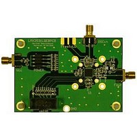
BOARD EVAL FOR LMX25311146
Manufacturer
National Semiconductor
Series
PowerWise®r
Datasheets
1.LMX2531LQ1778ENOPB.pdf
(36 pages)
2.LMX25311146EVAL.pdf
(23 pages)
3.LMX25311146EVAL.pdf
(34 pages)
Specifications of LMX25311146EVAL
Main Purpose
Timing, Frequency Synthesizer
Utilized Ic / Part
LMX2531LQ1146E
Silicon Manufacturer
National
Silicon Core Number
LMX2531
Kit Application Type
Clock & Timing
Application Sub Type
Frequency Synthesizer
Kit Contents
Board, Cable, CD
Lead Free Status / RoHS Status
Contains lead / RoHS non-compliant
Secondary Attributes
-
Embedded
-
Primary Attributes
-
Lead Free Status / Rohs Status
Supplier Unconfirmed


Symbol
Note 2: There are program bits that need to be set based on the OSCin frequency. Refer to the following sections: 2.7.8 XTLSEL[2:0] -- Crystal Select, 2.8.1
XTLDIV[1:0] -- Division Ratio for the Crystal Frequency, 2.8.2 XTLMAN[11:0] -- Manual Crystal Mode, 2.9.1 XTLMAN2 -- MANUAL CRYSTAL MODE SECOND
ADJUSTMENT, and2.9.2 LOCKMODE -- FREQUENCY CALIBRATION MODE. Not all bit settings can be used for all frequency choices of OSCin. For instance,
automatic modes described in 2.7.8 XTLSEL[2:0] -- Crystal Select do not work below 8 MHz.
Note 3: One of the specifications for modeling PLL in-band phase noise is the PLL 1/f noise normalized to 1 GHz carrier frequency and 10 kHz offset, L
(10 kHz). From this normalized index of PLL 1/f noise, the PLL 1/f noise can be calculated for any carrier and offset frequency as:
LN
slope and improves with higher charge pump currents and at higher offset frequencies . To accurately measure L
phase detector frequency and a clean reference to make it such that this measurement is on the 10 dB/decade slope close to the carrier. L
masked by the reference oscillator performance if a low power or noisy source is used. The total PLL in-band phase noise performance is the sum of L
(f) and L
Note 4: A specification used for modeling PLL in-band phase noise floor is the Normalized PLL noise floor, LN
LN
L
yet large enough to avoid a substantial noise contribution from the reference and PLL flicker noise. L
if a low power or noisy source is used. The total PLL in-band phase noise performance is the sum of L
words,L
Note 5: Maximum Allowable Temperature Drift for Continuous Lock is how far the temperature can drift in either direction from the value it was at the time that
the R0 register was last programmed, and still have the part stay in lock. The action of programming the R0 register, even to the same value, activates a frequency
calibration routine. This implies that the part will work over the entire frequency range, but if the temperature drifts more than the maximum allowable drift for
continuous lock, then it will be necessary to reload the R0 register to ensure that it stays in lock. Regardless of what temperature the part was initially programmed
at, the temperature can never drift outside the frequency range of -40°C
Note 6: The VCO phase noise is measured assuming that the loop bandwidth is sufficiently narrow that the VCO noise dominates. The maximum limits apply
only at center frequency and over temperature, assuming that the part is reloaded at each test frequency. Over frequency, the phase noise can vary 1 to 2 dB,
with the worst case performance typically occurring at the highest frequency. Over temperature, the phase noise typically varies 1 to 2 dB, assuming the part is
reloaded.
t
t
t
V
t
V
V
t
CWH
CWL
EWH
PLL_flat
V
t
t
CES
I
I
CH
CS
ES
IH
OH
IL
OL
PLL_flicker
PLL_flat
IH
IL
contributes to the total noise, L(f). To measure L
PLL
PLL_flat
= L(f) – 20·log(N) – 10·log(f
(f) = L
(f) = 10·log(10(
Clock to Enable Set Up Time
Enable to Clock Set Up Time
Data to Clock Set Up Time
High-Level Output Voltage
Low-Level Output Voltage
. In other words,L
High-Level Input Voltage
Enable Pulse Width High
High-Level Input Current
Data to Clock Hold Time
Low-Level Input Voltage
Low-Level Input Current
Clock Pulse Width High
Clock Pulse Width Low
PLL_flicker
Parameter
(10 kHz) - 10·log(10 kHz / f) + 20·log( Fout / 1 GHz ). Flicker noise can dominate at low offsets from the carrier and has a 10 dB/decade
LN
PLL_flat
PLL
/ 10 )
(f) = 10·log(10(
PD
+ 10(
). L
PLL_flat
LN
Digital Interface (DATA, CLK, LE, CE, Ftest/LD, FLout)
PLL_flicker
is the single side band phase noise in a 1 Hz Bandwidth and f
LN
(f) / 10 )
PLL_flat
PLL_flat
/ 10 )
+ 10(
the offset frequency must be chosen sufficiently smaller then the loop bandwidth of the PLL, and
LN
MICROWIRE Timing
PLL_flicker
See Data Input Timing
See Data Input Timing
See Data Input Timing
See Data Input Timing
See Data Input Timing
See Data Input Timing
See Data Input Timing
≤
(f) / 10 )
T
A
I
I
≤
Conditions
OL
OH
15
V
V
85°C without violating specifications.
IH
= -500 µA
IL
= 500 µA
= 1.75
= 0 V
PLL_flat
PLL_flicker
can be masked by the reference oscillator performance
PD
is the phase detector frequency of the synthesizer.
(f) and L
PLL_flat
PLL_flicker
, and is defined as:
PLL_flat
(10 kHz) it is important to use a high
Min
-3.0
-3.0
1.6
2.0
25
20
25
25
25
25
25
. In other
2.65
Typ
0.0
PLL_flicker
Max
2.75
0.4
3.0
3.0
0.4
www.national.com
(f) can be
PLL_flicker
PLL_flicker
Units
µA
µA
ns
ns
ns
ns
ns
ns
ns
V
V
V
V
Related parts for LMX25311146EVAL
Image
Part Number
Description
Manufacturer
Datasheet
Request
R

Part Number:
Description:
National Semiconductor [8-Bit D/A Converter]
Manufacturer:
National Semiconductor
Datasheet:
Part Number:
Description:
National Semiconductor [Media Coprocessor]
Manufacturer:
National Semiconductor
Datasheet:
Part Number:
Description:
Digitally Controlled Tone and Volume Circuit with Stereo Audio Power Amplifier, Microphone Preamp Stage and National 3D Sound
Manufacturer:
National Semiconductor
Datasheet:
Part Number:
Description:
Digitally Controlled Tone and Volume Circuit with Stereo Audio Power Amplifier, Microphone Preamp Stage and National 3D Sound
Manufacturer:
National Semiconductor
Datasheet:
Part Number:
Description:
AC97 Rev 2 Codec with Sample Rate Conversion and National 3D Sound
Manufacturer:
National Semiconductor
Part Number:
Description:
Manufacturer:
National Semiconductor
Datasheet:
Part Number:
Description:
Manufacturer:
National Semiconductor
Datasheet:
Part Number:
Description:
General Purpose, Low Voltage, Low Power, Rail-to-Rail Output Operational Amplifiers
Manufacturer:
National Semiconductor
Datasheet:
Part Number:
Description:
8-bit 20 MSPS flash A/D converter.
Manufacturer:
National Semiconductor
Datasheet:
Part Number:
Description:
Low Noise Quad Operational Amplifier
Manufacturer:
National Semiconductor
Datasheet:
Part Number:
Description:
Quad Differential Line Receivers
Manufacturer:
National Semiconductor
Datasheet:
Part Number:
Description:
Quad High Speed Trapezoidal? Bus Transceiver
Manufacturer:
National Semiconductor
Datasheet:
Part Number:
Description:
Dual Line Receiver
Manufacturer:
National Semiconductor
Datasheet:
Part Number:
Description:
TTL to 10k ECL Level Translator with Latch
Manufacturer:
National Semiconductor
Datasheet: