LMX25313010EVAL National Semiconductor, LMX25313010EVAL Datasheet - Page 28
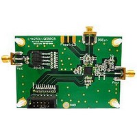
LMX25313010EVAL
Manufacturer Part Number
LMX25313010EVAL
Description
BOARD EVAL FOR LMX25131LQ 3010
Manufacturer
National Semiconductor
Series
PowerWise®r
Specifications of LMX25313010EVAL
Main Purpose
Timing, Frequency Synthesizer
Embedded
No
Utilized Ic / Part
LMX2531LQ3010
Primary Attributes
Low Band 1455 - 1566 MHz, High Band 2910 - 3132 MHz
Secondary Attributes
2.8 V ~ 3.2 V Supply
Silicon Manufacturer
National
Silicon Core Number
LMX2531
Kit Application Type
Clock & Timing
Application Sub Type
Frequency Synthesizer
Kit Contents
Board, Cable, CD
Lead Free Status / RoHS Status
Contains lead / RoHS non-compliant


2.6 REGISTER R5
2.6.1 EN_PLL -- Enable Bit for PLL
When this bit is set to 1 (default), the PLL is powered up, otherwise, it is powered down.
2.6.2 EN_VCO -- Enable Bit for the VCO
When this bit is set to 1 (default), the VCO is powered up, otherwise, it is powered down.
2.6.3 EN_OSC -- Enable Bit for the Oscillator Inverter
When this bit is set to 1 (default), the reference oscillator is powered up, otherwise it is powered down.
2.6.4 EN_VCOLDO -- Enable Bit for the VCO LDO
When this bit is set to 1 (default), the VCO LDO is powered up, otherwise it is powered down.
2.6.5 EN_PLLLDO1 -- Enable Bit for the PLL LDO 1
When this bit is set to 1 (default), the PLL LDO 1 is powered up, otherwise it is powered down.
2.6.6 EN_PLLLDO2 -- Enable Bit for the PLL LDO 2
When this bit is set to 1 (default), the PLL LDO 2 is powered up, otherwise it is powered down.
2.6.7 EN_DIGLDO -- Enable Bit for the digital LDO
When this bit is set to 1 (default), the Digital LDO is powered up, otherwise it is powered down.
2.6.8 REG_RST -- RESETS ALL REGISTERS TO DEFAULT SETTINGS
This bit needs to be programmed three times to initialize the part. When this bit is set to one, all registers are set to default mode,
and the part is powered down. The second time the R5 register is programmed with REG_RST=0, the register reset is released
and the default states are still in the registers. However, since the default states for the blocks and LDOs is powered off, it is
therefore necessary to program R5 a third time so that all the LDOs and blocks can be programmed to a power up state. When
this bit is set to 1, all registers are set to the default modes, but part is powered down. For normal operation, this bit is set to 0.
Note that once this initialization is done, it is not necessary to do this again unless power is removed from the device.
www.national.com
28
Related parts for LMX25313010EVAL
Image
Part Number
Description
Manufacturer
Datasheet
Request
R

Part Number:
Description:
National Semiconductor [8-Bit D/A Converter]
Manufacturer:
National Semiconductor
Datasheet:
Part Number:
Description:
National Semiconductor [Media Coprocessor]
Manufacturer:
National Semiconductor
Datasheet:
Part Number:
Description:
Digitally Controlled Tone and Volume Circuit with Stereo Audio Power Amplifier, Microphone Preamp Stage and National 3D Sound
Manufacturer:
National Semiconductor
Datasheet:
Part Number:
Description:
Digitally Controlled Tone and Volume Circuit with Stereo Audio Power Amplifier, Microphone Preamp Stage and National 3D Sound
Manufacturer:
National Semiconductor
Datasheet:
Part Number:
Description:
AC97 Rev 2 Codec with Sample Rate Conversion and National 3D Sound
Manufacturer:
National Semiconductor
Part Number:
Description:
Manufacturer:
National Semiconductor
Datasheet:
Part Number:
Description:
Manufacturer:
National Semiconductor
Datasheet:
Part Number:
Description:
General Purpose, Low Voltage, Low Power, Rail-to-Rail Output Operational Amplifiers
Manufacturer:
National Semiconductor
Datasheet:
Part Number:
Description:
8-bit 20 MSPS flash A/D converter.
Manufacturer:
National Semiconductor
Datasheet:
Part Number:
Description:
Low Noise Quad Operational Amplifier
Manufacturer:
National Semiconductor
Datasheet:
Part Number:
Description:
Quad Differential Line Receivers
Manufacturer:
National Semiconductor
Datasheet:
Part Number:
Description:
Quad High Speed Trapezoidal? Bus Transceiver
Manufacturer:
National Semiconductor
Datasheet:
Part Number:
Description:
Dual Line Receiver
Manufacturer:
National Semiconductor
Datasheet:
Part Number:
Description:
TTL to 10k ECL Level Translator with Latch
Manufacturer:
National Semiconductor
Datasheet: