NCP370GEVB ON Semiconductor, NCP370GEVB Datasheet - Page 3
NCP370GEVB
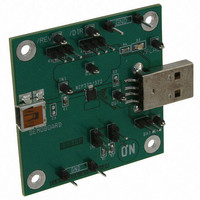
Manufacturer Part Number
NCP370GEVB
Description
EVAL BOARD FOR NCP370G
Manufacturer
ON Semiconductor
Specifications of NCP370GEVB
Design Resources
NCP370GEVB BOM NCP370GEVB Gerber Files NCP370GEVB Schematic
Main Purpose
Overvoltage Protection
Embedded
No
Utilized Ic / Part
NCP370
Primary Attributes
Overvoltage Protected up to 28V and down to -28V
Secondary Attributes
Reverse Mode
Lead Free Status / RoHS Status
Lead free / RoHS Compliant
For Use With/related Products
NCP370G
Other names
NCP370GEVBOS


Stresses exceeding Maximum Ratings may damage the device. Maximum Ratings are stress ratings only. Functional operation above the
Recommended Operating Conditions is not implied. Extended exposure to stresses above the Recommended Operating Conditions may affect
device reliability.
1. The R
2. Human Body Model, 100 pF discharged through a 1.5 kW resistor following specification JESD22/A114.
3. Machine Model, 200 pF discharged through all pins following specification JESD22/A115.
Maximum Voltage (IN to GND)
Maximum Voltage (OUT to GND)
Maximum Voltage (All others to GND)
PIN FUNCTION DESCRIPTION
MAXIMUM RATINGS
Minimum Voltage (IN to GND)
Minimum Voltage (All others to GND)
Thermal Resistance, Junction−to−Air, (Note 1)
Operating Ambient Temperature Range
Storage Temperature Range
Junction Operating Temperature
ESD Withstand Voltage (IEC 61000−4−2)
Human Body Model (HBM), Model = 2, (Note 2)
Machine Model (MM) Model = B, (Note 3)
Moisture Sensitivity
1, 2
Pin
10
11
12
13
3
4
5
6
7
8
9
qJA
Name
FLAG
PAD1
GND
OUT
RES
RES
RES
REV
DIR
Ilim
NC
IN
is highly dependent on the PCB heat sink area (connected to PAD1). See PCB recommendation paragraph.
OUTPUT
OUTPUT
OUTPUT
POWER
POWER
POWER
INPUT
INPUT
INPUT
INPUT
INPUT
Type
NC
Input voltage pins. These pins are connected to the power supply. A 1 mF low ESR ceramic capacitor, or
larger, must be connected between these pins and GND. The two IN pins must be hardwired to common
supply.
Main Ground
Reserved pin. This pin must be connected to GND.
Reserved pin. This pin must be connected to GND.
Reserved pin. This pin must be connected to GND.
Current Limit Pin. This pin provides the reference, based on the internal band−gap voltage reference, to
limit the over current, across internal N−MOSFETs, from battery to external accessory. A 1% tolerance,
or better, resistor shall be used to get the highest accuracy of the overcurrent limit.
Reverse Charge Control Pin. In combination with DIR, the internal N−MOSFETs are turned on if Battery
is applied on the OUT pin (See Tables 1 & 2). In reverse mode, the internal overcurrent protection is
activated. When reverse mode is disabled, the NCP370 current consumption, into OUT pin, is drastically
decreased to limit battery discharge.
Direct Mode Pin. In combination with REV, the internal N−MOSFETs are turned on if a wall adapter
AC−DC is applied on the IN pins (See Tables 1 & 2). The device enters in shutdown mode when this pin
is tied to a high level and the REV pin is tied to high. In this case the output is disconnected from input.
The state of this pin does not have an impact on the fault detect of the FLAG pin.
Fault Indication Pin. This pin allows an external system to detect fault condition. The pin goes low when
input voltage exceeds OVLO threshold or drops below UVLO threshold, charge current from battery to
accessory exceeds current limit or internal temperature exceeds thermal shutdown limit. Since the pin is
open drain functionality, an external pull up resistor to VBat must be added (10 kW minimum value).
Output Voltage Pin. This pin follows IN pins when “no input fault” is detected. The output is disconnected
from the V
or thermal shutdown limit is exceeded.In Reverse Mode, the device is supplied across OUT pin.
Not Connected
The PAD1 is used to dissipate the internal MOSFET thermal energy and must be soldered to an isolated
PCB area. The area mustn’t be connected to any other potential than complete isolated one. See PCB
recommendations on page 9.
Rating
IN
power supply when the input voltage is under the UVLO threshold or above OVLO threshold
http://onsemi.com
3
Description
Symbol
Vmax
Vmax
Vmin
Vmax
Vmin
T
Vesd
R
MSL
T
STG
T
qJA
A
J
out
in
in
15kV air, 8kV contact
−65 to +150
−40 to +85
Level 1
2000V
Value
200V
−0.3
−30
200
150
30
10
7
°C/W
Unit
°C
°C
°C
kV
V
V
V
V
V
V
V
Related parts for NCP370GEVB
Image
Part Number
Description
Manufacturer
Datasheet
Request
R

Part Number:
Description:
Positive and Negative Overvoltage Protection
Manufacturer:
ON Semiconductor
Datasheet:
Part Number:
Description:
ON Semiconductor [VOLTAGE REGULATOR]
Manufacturer:
ON Semiconductor
Datasheet:
Part Number:
Description:
357-036-542-201 CARDEDGE 36POS DL .156 BLK LOPRO
Manufacturer:
ON Semiconductor
Datasheet:
Part Number:
Description:
357-036-542-201 CARDEDGE 36POS DL .156 BLK LOPRO
Manufacturer:
ON Semiconductor
Datasheet:
Part Number:
Description:
357-036-542-201 CARDEDGE 36POS DL .156 BLK LOPRO
Manufacturer:
ON Semiconductor
Datasheet:
Part Number:
Description:
357-036-542-201 CARDEDGE 36POS DL .156 BLK LOPRO
Manufacturer:
ON Semiconductor
Datasheet:
Part Number:
Description:
357-036-542-201 CARDEDGE 36POS DL .156 BLK LOPRO
Manufacturer:
ON Semiconductor
Datasheet:
Part Number:
Description:
357-036-542-201 CARDEDGE 36POS DL .156 BLK LOPRO
Manufacturer:
ON Semiconductor
Datasheet:
Part Number:
Description:
357-036-542-201 CARDEDGE 36POS DL .156 BLK LOPRO
Manufacturer:
ON Semiconductor
Datasheet:
Part Number:
Description:
357-036-542-201 CARDEDGE 36POS DL .156 BLK LOPRO
Manufacturer:
ON Semiconductor
Datasheet:
Part Number:
Description:
357-036-542-201 CARDEDGE 36POS DL .156 BLK LOPRO
Manufacturer:
ON Semiconductor
Datasheet:
Part Number:
Description:
357-036-542-201 CARDEDGE 36POS DL .156 BLK LOPRO
Manufacturer:
ON Semiconductor
Datasheet:
Part Number:
Description:
Manufacturer:
ON Semiconductor
Datasheet:
Part Number:
Description:
Manufacturer:
ON Semiconductor
Datasheet: