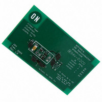
AND8203/D
Simple Input Adapter
Reverse Voltage Protection
Prepared by: Jim Hill
ON Semiconductor
regulated voltages to power various subsystems. The
number of voltage rails has risen as new generations of
processors, memory, etc. have been introduced with lower
voltage requirements driven by deep sub−micron CMOS
processes. One of the consequences of these new process
technologies is that the absolute maximum ratings have also
been lowered, therefore designers are forced to employ
protection circuitry to protect sensitive I/O’s from transient
and steady−state overvoltage and reverse voltage
conditions.
result in overvoltage events that can damage sensitive
electronic components within the product. Also, due to the
proliferation of portable products within the home and
office, a risk exists that the user may reach for the wrong
adapter which could have a reversed polarity. The challenge
of the product designer is to improve the robustness of the
design and avoid situations where the product can be
damaged.
any reverse current into the adapter. However, Schottky
diodes have a forward voltage drop, V
depending on the forward current, I
have maximum voltage of 4.2 V. Finally, adapter voltages
© Semiconductor Components Industries, LLC, 2005
March, 2005 − Rev. 0
Modern electronic systems require a host of different
Failures and faults in the adapter may, and usually do,
A series Schottky will clamp the reverse voltage and block
V
+
−
in
Q2
(Optional)
Figure 1. NCP345/6 Circuit with Reverse Input Voltage Protection
(Optional)
F
. Next, Li−Ion batteries
IN
GND
F
, from 0.3−0.5 V
+
−
+
−
V
ref
V
CC
Logic
1
Microprocessor port
CNTRL
are falling due to the standardization of single−cell Li−Ion
as a portable power source, and by lowering the adapter
output voltage, the output power is reduced and thus the size
and cost of the adapter. So in many cases, there is not enough
voltage headroom to support the addition of a Schottky to
provide reverse clamping.
transients up to 30 V and steady state overvoltage faults of
25 V while allowing normal operation for low voltage
adapter inputs. The NCP345/6 senses an overvoltage
condition and quickly disconnects the input voltage supply
from the load by turning off Q1. The NCP345 senses
overvoltage events greater than 6.85 V and the NCP346
comes in two versions which detect overvoltage events
greater than 4.45 and 5.5 V respectively. An optional
resistor divider may be used to adjust the detection threshold
to a higher value as well. Transistor Q2 protects the circuit
from a reverse input voltage condition. For a correct, or
positive, input voltage (V
rises above the body diode voltage of the transistor. The
body diode polarity allows the source to pull up to the input
voltage which turns on the transistor and shorts out the
diode. For a reversed V
is not allowed to turn on.
NCP345/6
The circuit in Figure 1 protects its output from input
Driver
FET
OUT
Q1
APPLICATION NOTE
in
, since the gate is grounded, the FET
http://onsemi.com
in
), the transistor turns on once V
D1
Publication Order Number:
+
C1
AND8203/D
LOAD
in


