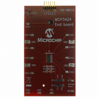
MCP3424EV Microchip Technology, MCP3424EV Datasheet - Page 11
MCP3424EV
Manufacturer Part Number
MCP3424EV
Description
EVALUATION BOARD FOR MCP3424
Manufacturer
Microchip Technology
Specifications of MCP3424EV
Number Of Adc's
1
Number Of Bits
18
Sampling Rate (per Second)
3.75 ~ 240
Data Interface
I²C
Inputs Per Adc
4 Differential
Input Range
±2.048 V
Power (typ) @ Conditions
135µA @ 240sps
Voltage Supply Source
Single Supply
Operating Temperature
-55°C ~ 125°C
Utilized Ic / Part
MCP3424
Processor To Be Evaluated
MCP3424
Lead Free Status / RoHS Status
Lead free / RoHS Compliant
Lead Free Status / RoHS Status
Lead free / RoHS Compliant, Lead free / RoHS Compliant
Available stocks
Company
Part Number
Manufacturer
Quantity
Price
Company:

Part Number:
MCP3424EV
Manufacturer:
Microchip Technology
Quantity:
135


4.5
The differential (V
(V
setting are defined by:
The input signal levels are amplified by the internal
programmable gain amplifier (PGA) at the front end of
the ΔΣ modulator.
The user needs to consider two conditions for the input
voltage range: (a) Differential input voltage range and
(b) Absolute input voltage range.
4.5.1
The device performs conversions using its internal
reference voltage (V
absolute value of the differential input voltage (V
with PGA setting is included, needs to be less than the
internal reference voltage. The device will output satu-
rated output codes (all 0s or all 1s except sign bit ) if the
absolute value of the input voltage (V
setting is included, is greater than the internal
reference voltage (V
voltage range is given by:
EQUATION 4-1:
If the input voltage level is greater than the above limit,
the user can use a voltage divider and bring down the
input level within the full-scale range. See
for more details of the input voltage divider circuit.
4.5.2
The input voltage at each input pin must be less than
the following absolute maximum input voltage limits:
• Input voltage < V
• Input voltage > V
Any input voltage outside this range can turn on the
input ESD protection diodes, and result in input leak-
age current, causing conversion errors, or permanently
damage the device.
Care must be taken in setting the input voltage ranges
so that the input voltage does not exceed the absolute
maximum input voltage range.
© 2008 Microchip Technology Inc.
Where:
Where:
INCOM
V
REF
V
IN
n
) at the input pins without considering PGA
–
Input Voltage Range
V
REF
Differential Input Voltage Range
V
Absolute Maximum Input Voltage Range:
=
INCOM
=
=
V
≤
IN
(
V
nth input channel (n=1, 2, 3, or 4)
=
IN
DD
SS
IN
CHn+ - CHn-
2.048V
REF
=
) and common mode voltage
•
-0.3V
(
+0.3V
REF
CHn+
PGA
(
---------------------------------------------- -
= 2.048V). The input full-scale
CHn+
= 2.048V). Therefore, the
)
)
≤
–
)
(
(
2
V
+
CHn-
REF
(
CHn-
–
)
1LSB
IN
)
), with PGA
Figure 6-6
)
IN
),
4.6
The MCP3424 uses a switched-capacitor input stage
using a 3.2 pF sampling capacitor. This capacitor is
switched (charged and discharged) at a rate of the
sampling frequency that is generated by on-board
clock. The differential input impedance varies with the
PGA settings. The typical differential input impedance
during a normal mode operation is given by:
Since the sampling capacitor is only switching to the
input pins during a conversion process, the above input
impedance is only valid during conversion periods. In a
low power standby mode, the above impedance is not
presented at the input pins. Therefore, only a leakage
current due to ESD diode is presented at the input pins.
The conversion accuracy can be affected by the input
signal source impedance when any external circuit is
connected to the input pins. The source impedance
adds to the internal impedance and directly affects the
time required to charge the internal sampling capacitor.
Therefore, a large input source impedance connected
to the input pins can degrade the system performance,
such as offset, gain, and Integral Non-Linearity (INL)
errors. Ideally, the input source impedance should be
zero. This can be achievable by using an operational
amplifier with a closed-loop output impedance of tens
of ohms.
4.7
Aliasing occurs when the input signal contains
time-varying signal components with frequency greater
than half the sample rate. In the aliasing conditions, the
device can output unexpected output codes. For
applications that are operating in electrical noise
environments, the time-varying signal noise or high
frequency interference components can be easily
added to the input signals and cause aliasing. Although
the MCP3424 device has an internal first order sinc
filter, its filter response
enough attenuation to all aliasing signal components.
To avoid the aliasing, an external anti-aliasing filter,
which can be accomplished with a simple RC low-pass
filter, is typically used at the input pins. The low-pass
filter cuts off the high frequency noise components and
provides a band-limited input signal to the MCP3424
input pins.
4.8
The device performs a self-calibration of offset and
gain for each conversion. This provides reliable
conversion results from conversion-to-conversion over
variations in temperature as well as power supply
fluctuations.
Aliasing and Anti-aliasing Filter
Input Impedance
Self-Calibration
Z
IN
(f) = 2.25 M
(Figure
MCP3424
Ω
/PGA
2-11) may not give
DS22088A-page 11
Related parts for MCP3424EV
Image
Part Number
Description
Manufacturer
Datasheet
Request
R

Part Number:
Description:
Manufacturer:
Microchip Technology Inc.
Datasheet:
Part Number:
Description:
Manufacturer:
Microchip Technology Inc.
Datasheet:
Part Number:
Description:
Manufacturer:
Microchip Technology Inc.
Datasheet:
Part Number:
Description:
Manufacturer:
Microchip Technology Inc.
Datasheet:
Part Number:
Description:
Manufacturer:
Microchip Technology Inc.
Datasheet:
Part Number:
Description:
Manufacturer:
Microchip Technology Inc.
Datasheet:
Part Number:
Description:
Manufacturer:
Microchip Technology Inc.
Datasheet:
Part Number:
Description:
Manufacturer:
Microchip Technology Inc.
Datasheet: