MCP3424EV Microchip Technology, MCP3424EV Datasheet - Page 16
MCP3424EV
Manufacturer Part Number
MCP3424EV
Description
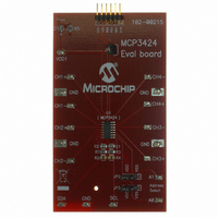
EVALUATION BOARD FOR MCP3424
Manufacturer
Microchip Technology
Specifications of MCP3424EV
Number Of Adc's
1
Number Of Bits
18
Sampling Rate (per Second)
3.75 ~ 240
Data Interface
I²C
Inputs Per Adc
4 Differential
Input Range
±2.048 V
Power (typ) @ Conditions
135µA @ 240sps
Voltage Supply Source
Single Supply
Operating Temperature
-55°C ~ 125°C
Utilized Ic / Part
MCP3424
Processor To Be Evaluated
MCP3424
Lead Free Status / RoHS Status
Lead free / RoHS Compliant
Lead Free Status / RoHS Status
Lead free / RoHS Compliant, Lead free / RoHS Compliant
Available stocks
Company
Part Number
Manufacturer
Quantity
Price
Company:

Part Number:
MCP3424EV
Manufacturer:
Microchip Technology
Quantity:
135


MCP3422/3/4
4.9.2
When the user gets the digital output codes from the
device as described in Section 4.9.1 “Digital output
code from device”, the next step is converting the
digital output codes to a measured input voltage.
Equation 4-4
output codes to its corresponding input voltage.
If the sign indicator bit (MSB) is ‘0’, the input voltage
is obtained by multiplying the output code with the LSB
and divided by the PGA setting.
If the sign indicator bit (MSB) is ‘1’, the output code
needs to be converted to two’s complement before
multiplied by LSB and divided by the PGA setting.
Table 4-4
output codes to input voltage.
TABLE 4-4:
DS22088C-page 16
[CHn+ - CHn-]
Input Voltage
V
REF
≤ -V
≥ V
-1 LSB
-2 LSB
- V
2 LSB
1 LSB
- 1 LSB
shows an example of converting the device
0
REF
REF
REF
CONVERTING THE DEVICE
OUTPUT CODE TO INPUT SIGNAL
VOLTAGE
shows an example of converting the
•
PGA]
EXAMPLE OF CONVERTING OUTPUT CODE TO VOLTAGE (WITH 18 BIT SETTING)
011111111111111111
011111111111111111
000000000000000010
000000000000000001
000000000000000000
111111111111111111
111111111111111110
100000000000000000
100000000000000000
Digital Output Code
MSB
0
0
0
0
0
1
1
1
1
(2
x LSB(15.625μV)/PGA = 2.048 (V) for PGA = 1
(2
x LSB(15.625μV)/PGA = 2.048 (V) for PGA = 1
(0+0+0+0+0+0+0+0+0+0+0+0+0+0+0+2
= 31.25 (μV) for PGA = 1
(0+0+0+0+0+0+0+0+0+0+0+0+0+0+0+0+2
= 15.625 (μV)for PGA = 1
(0+0+0+0+0+0+0+0+0+0+0+0+0+0+0+0+0)x LSB(15.625μV)/PGA
= 0 V (V) for PGA = 1
-(0+0+0+0+0+0+0+0+0+0+0+0+0+0+0+0+2
= - 15.625 (μV)for PGA = 1
-(0+0+0+0+0+0+0+0+0+0+0+0+0+0+0+2
= - 31.25 (μV)for PGA = 1
-(2
LSB(15.625μV)/PGA = - 2.048 (V) for PGA = 1
-(2
LSB(15.625μV)/PGA = - 2.048 (V) for PGA = 1
16
16
17
17
+2
+2
+0+0+0+0+0+0+0+0+0+0+0+0+0+0+0+0+0) x
+0+0+0+0+0+0+0+0+0+0+0+0+0+0+0+0+0) x
15
15
Example of Converting Output Codes to Input Voltage
+2
+2
14
14
+2
+2
EQUATION 4-4:
Where:
If MSB = 0 (Positive Output Code):
If MSB = 1 (Negative Output Code):
13
13
2’s complement
Input Voltage
+2
+2
12
12
+2
+2
Input Voltage
11
11
+2
+2
LSB
10
10
=
+2
+2
(2
9
9
′
+2
+2
s complement of Output Code)
=
=
=
CONVERTING OUTPUT
CODES TO INPUT
VOLTAGE
8
8
+2
+2
© 2009 Microchip Technology Inc.
(Output Code)
1
7
7
+0)x LSB(15.625μV)/PGA
1
See
1’s complement + 1
+2
+2
+0)x LSB(15.625μV)/PGA
0
)x LSB(15.625μV)/PGA
0
6
6
)x LSB(15.625μV)/PGA
+2
+2
Table 4-1
5
5
+2
+2
4
4
+2
+2
•
3
3
----------- -
PGA
LSB
+2
+2
2
2
+2
+2
1
1
•
+2
+2
----------- -
PGA
LSB
0
0
)
)
Related parts for MCP3424EV
Image
Part Number
Description
Manufacturer
Datasheet
Request
R

Part Number:
Description:
Manufacturer:
Microchip Technology Inc.
Datasheet:
Part Number:
Description:
Manufacturer:
Microchip Technology Inc.
Datasheet:
Part Number:
Description:
Manufacturer:
Microchip Technology Inc.
Datasheet:
Part Number:
Description:
Manufacturer:
Microchip Technology Inc.
Datasheet:
Part Number:
Description:
Manufacturer:
Microchip Technology Inc.
Datasheet:
Part Number:
Description:
Manufacturer:
Microchip Technology Inc.
Datasheet:
Part Number:
Description:
Manufacturer:
Microchip Technology Inc.
Datasheet:
Part Number:
Description:
Manufacturer:
Microchip Technology Inc.
Datasheet: