MCP3423EV Microchip Technology, MCP3423EV Datasheet - Page 18
MCP3423EV
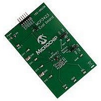
Manufacturer Part Number
MCP3423EV
Description
BOARD EVAL 18BIT 2CH ADC MCP3423
Manufacturer
Microchip Technology
Specifications of MCP3423EV
Number Of Adc's
1
Number Of Bits
18
Sampling Rate (per Second)
3.75
Data Interface
Serial
Inputs Per Adc
2 Differential
Input Range
±VREF
Voltage Supply Source
Single Supply
Operating Temperature
-40°C ~ 125°C
Utilized Ic / Part
MCP3423
Silicon Manufacturer
Microchip
Application Sub Type
ADC
Kit Application Type
Data Converter
Silicon Core Number
MCP3423
Lead Free Status / RoHS Status
Lead free / RoHS Compliant


MCP3422/3/4
5.2
The device has an 8-bit wide configuration register to
select for: input channel, conversion mode, conversion
rate, and PGA gain. This register allows the user to
change the operating condition of the device and check
the status of the device operation.
REGISTER 5-1:
DS22088C-page 18
bit 7
* Default Configuration after Power-On Reset
Legend:
R = Readable bit
-n = Value at POR
bit 7
bit 6-5
bit 4
bit 3-2
bit 1-0
R/W-1
RDY
1 *
Configuration Register
RDY: Ready Bit
This bit is the data ready flag. In read mode, this bit indicates if the output register has been updated
with a latest conversion result. In One-Shot Conversion mode, writing this bit to “1” initiates a new
conversion.
Reading RDY bit with the read command:
1 = Output register has not been updated
0 = Output register has been updated with the latest conversion result
Writing RDY bit with the write command:
Continuous Conversion mode: No effect
One-Shot Conversion mode:
1 = Initiate a new conversion
0 = No effect
C1-C0: Channel Selection Bits
00 =
01 =
10 =
11 =
O/C: Conversion Mode Bit
1 = Continuous Conversion Mode (Default). The device performs data conversions continuously
0 = One-Shot Conversion Mode. The device performs a single conversion and enters a low power
S1-S0: Sample Rate Selection Bit
00 =
01 =
10 =
11 =
G1-G0: PGA Gain Selection Bits
00 =
01 =
10 =
11 =
R/W-0
standby mode until it receives another write or read command
C1
0 *
CONFIGURATION REGISTER
Select Channel 1 (Default)
Select Channel 2
Select Channel 3 (MCP3424 only, treated as “00” by the MCP3422/MCP3423)
Select Channel 4 (MCP3424 only, treated as “01” by the MCP3422/MCP3423)
240 SPS (12 bits) (Default)
60 SPS (14 bits)
15 SPS (16 bits)
3.75 SPS (18 bits)
x1 (Default)
x2
x4
x8
W = Writable bit
‘1’ = Bit is set
R/W-0
C0
0 *
R/W-1
O/C
1 *
U = Unimplemented bit, read as ‘0’
‘0’ = Bit is cleared
R/W-0
The user can rewrite the configuration byte any time
during the device operation. Register 5-1 shows the
configuration register bits.
0 *
S1
R/W-0
S0
0 *
© 2009 Microchip Technology Inc.
x = Bit is unknown
R/W-0
G1
0 *
R/W-0
G0
0 *
bit 0
Related parts for MCP3423EV
Image
Part Number
Description
Manufacturer
Datasheet
Request
R

Part Number:
Description:
Manufacturer:
Microchip Technology Inc.
Datasheet:
Part Number:
Description:
Manufacturer:
Microchip Technology Inc.
Datasheet:
Part Number:
Description:
Manufacturer:
Microchip Technology Inc.
Datasheet:
Part Number:
Description:
Manufacturer:
Microchip Technology Inc.
Datasheet:
Part Number:
Description:
Manufacturer:
Microchip Technology Inc.
Datasheet:
Part Number:
Description:
Manufacturer:
Microchip Technology Inc.
Datasheet:
Part Number:
Description:
Manufacturer:
Microchip Technology Inc.
Datasheet:
Part Number:
Description:
Manufacturer:
Microchip Technology Inc.
Datasheet: