MCP3909EV-MCU16 Microchip Technology, MCP3909EV-MCU16 Datasheet - Page 17
MCP3909EV-MCU16
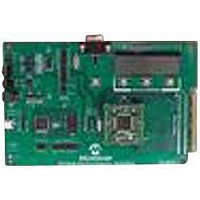
Manufacturer Part Number
MCP3909EV-MCU16
Description
EVALUATION BOARD FOR MCP3909
Manufacturer
Microchip Technology
Datasheets
1.MCP3909T-ISS.pdf
(44 pages)
2.MCP3909T-ISS.pdf
(104 pages)
3.MCP3909EV-MCU16.pdf
(38 pages)
Specifications of MCP3909EV-MCU16
Number Of Adc's
2
Number Of Bits
16
Sampling Rate (per Second)
15k
Data Interface
Serial
Inputs Per Adc
1 Differential
Input Range
±1 V
Voltage Supply Source
Analog and Digital
Operating Temperature
-40°C ~ 85°C
Utilized Ic / Part
MCP3909
Silicon Manufacturer
Microchip
Application Sub Type
ADC
Kit Application Type
Data Converter
Silicon Core Number
MCP3909
Kit Contents
Board
Lead Free Status / RoHS Status
Lead free / RoHS Compliant


3.14
This dual function pin can act as either the serial data
output for SPI communication or NEG. NEG detects the
phase difference between the two channels and will go
to a logic ‘1’ state when the phase difference is greater
than 90° (i.e., when the measured real power is
negative). The output state is synchronous with the
rising-edge of HF
the real power becomes positive again and HF
shows a pulse.
3.15
D
circuitry
digital-to-frequency converter and oscillator). To
ensure accuracy and noise cancellation, D
connected to the same ground as A
with a star connection. If a digital ground plane is
available, it is recommended that this device be tied to
this plane of the Printed Circuit Board (PCB). This
plane should also reference all other digital circuitry in
the system.
© 2009 Microchip Technology Inc.
GND
is the ground connection to internal digital
Serial Data Output or Negative
Power Output Logic Pin (NEG)
Ground Connection (D
(SINC
OUT
filters,
and maintains the logic ‘1’ until
multiplier,
GND
GND
HPF,
GND
, preferably
)
must be
LPF,
OUT
3.16
HF
supplies the instantaneous real-power information. The
output is a periodic pulse output, with its period propor-
tional to the measured real power, and to the HF
constant defined by F0, F1 and F2 pin logic states. This
output is the preferred output for calibration due to
faster output frequencies, giving smaller calibration
times. Since this output gives instantaneous real
power, the 2ω ripple on the output should be noted.
However, the average period will show minimal drift.
3.17
F
device that supply the average real-power information.
The outputs are periodic pulse outputs, with its period
proportional to the measured real power, and to the F
constant, defined by F0 and F1 pin logic states. These
pins include high-output drive capability for direct use
of electromechanical counters and 2-phase stepper
motors. Since this output supplies average real power,
any 2ω ripple on the output pulse period is minimal.
OUT0
OUT
and F
is the high-frequency output of the device and
High-Frequency Output (HF
Frequency Output (F
OUT1
are the frequency outputs of the
MCP3909
OUT0
DS22025B-page 17
, F
OUT
OUT1
)
)
C
C
Related parts for MCP3909EV-MCU16
Image
Part Number
Description
Manufacturer
Datasheet
Request
R

Part Number:
Description:
Manufacturer:
Microchip Technology Inc.
Datasheet:
Part Number:
Description:
Manufacturer:
Microchip Technology Inc.
Datasheet:
Part Number:
Description:
Manufacturer:
Microchip Technology Inc.
Datasheet:
Part Number:
Description:
Manufacturer:
Microchip Technology Inc.
Datasheet:
Part Number:
Description:
Manufacturer:
Microchip Technology Inc.
Datasheet:
Part Number:
Description:
Manufacturer:
Microchip Technology Inc.
Datasheet:
Part Number:
Description:
Manufacturer:
Microchip Technology Inc.
Datasheet:
Part Number:
Description:
Manufacturer:
Microchip Technology Inc.
Datasheet: