AD7940-DBRD Analog Devices Inc, AD7940-DBRD Datasheet - Page 15
AD7940-DBRD
Manufacturer Part Number
AD7940-DBRD
Description
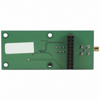
BOARD EVAL FOR AD7940 STAMP SPI
Manufacturer
Analog Devices Inc
Datasheet
1.AD7940BRJZ-REEL7.pdf
(20 pages)
Specifications of AD7940-DBRD
Number Of Adc's
1
Number Of Bits
14
Sampling Rate (per Second)
100k
Data Interface
Serial
Inputs Per Adc
1 Single Ended
Input Range
0 ~ Vdd
Power (typ) @ Conditions
17mW @ 100kSPS & 5 V
Voltage Supply Source
Single Supply
Operating Temperature
-40°C ~ 85°C
Utilized Ic / Part
AD7940
Lead Free Status / RoHS Status
Lead free / RoHS non-compliant


POWER VS. THROUGHPUT RATE
By using the power-down mode on the AD7940 when not
converting, the average power consumption of the ADC
decreases at lower throughput rates. Figure 19 shows how as the
throughput rate is reduced, the part remains in its shutdown
state longer, and the average power consumption over time
drops accordingly.
For example, if the AD7940 is operated in a continuous sam-
pling mode, with a throughput rate of 10 kSPS and an SCLK of
2.5 MHz (V
mode between conversions, the power consumption is calcu-
lated as follows. The maximum power dissipation during nor-
mal operation is 6.84 mW (V
from power-down is 1 µs, and the remaining conversion time is
6.4 µs, (using a 16 SCLK transfer), then the AD7940 can be said
to dissipate 6.84 mW for 7.4 µs during each conversion cycle.
With a throughput rate of 10 kSPS, the cycle time is 100 µs. For
the remainder of the conversion cycle, 92.6 µs, the part remains
in power-down mode. The AD7940 can be said to dissipate
1.08 µW for the remaining 92.6 µs of the conversion cycle.
Therefore, with a throughput rate of 10 kSPS, the average power
dissipated during each cycle is
(7.4/100) × (6.84 mW) + (92.6/100) × (1.08 µW) = 0.51 mW
DD
= 3.6 V), and the device is placed in power-down
DD
= 3.6 V). If the power-up time
Rev. 0 | Page 15 of 20
Figure 19 shows the power dissipation versus the throughput
rate when using the power-down mode with 3.6 V supplies and
a 2.5 MHz SCLK.
Figure 19. Power vs. Throughput Using Power-Down Mode at 3.6 V
0.01
0.1
10
1
0
V
F
DD
SCLK
= 3.6V
5
= 2.5MHz
10
15
THROUGHPUT (kSPS)
20
25
30
35
40
45
AD7940
50
Related parts for AD7940-DBRD
Image
Part Number
Description
Manufacturer
Datasheet
Request
R

Part Number:
Description:
±1.7g Dual-Axis IMEMS Accelerometer Evaluation Board
Manufacturer:
Analog Devices Inc
Datasheet:

Part Number:
Description:
Inertial Sensor Evaluation System
Manufacturer:
Analog Devices Inc
Datasheet:
Part Number:
Description:
Manufacturer:
Analog Devices Inc
Datasheet:
Part Number:
Description:
Manufacturer:
Analog Devices Inc
Datasheet:
Part Number:
Description:
Manufacturer:
Analog Devices Inc
Datasheet:
Part Number:
Description:
Manufacturer:
Analog Devices Inc
Datasheet:
Part Number:
Description:
Manufacturer:
Analog Devices Inc
Datasheet:
Part Number:
Description:
Manufacturer:
Analog Devices Inc
Datasheet:
Part Number:
Description:
Manufacturer:
Analog Devices Inc
Datasheet:
Part Number:
Description:
Manufacturer:
Analog Devices Inc
Datasheet:
Part Number:
Description:
Manufacturer:
Analog Devices Inc
Datasheet:
Part Number:
Description:
Manufacturer:
Analog Devices Inc
Datasheet:
Part Number:
Description:
Manufacturer:
Analog Devices Inc
Datasheet: