CDB5571 Cirrus Logic Inc, CDB5571 Datasheet - Page 16
CDB5571
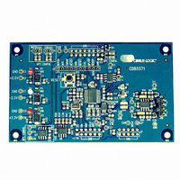
Manufacturer Part Number
CDB5571
Description
DEV BOARD FOR CS5571 W/MUX
Manufacturer
Cirrus Logic Inc
Type
A/Dr
Specifications of CDB5571
Number Of Adc's
1
Number Of Bits
16
Sampling Rate (per Second)
100k
Data Interface
Serial
Inputs Per Adc
2 Single
Input Range
2.4 ~ 4.2 V
Voltage Supply Source
Dual ±
Operating Temperature
-40°C ~ 85°C
Utilized Ic / Part
CS5571
Product
Data Conversion Development Tools
Conversion Rate
100 KSPS
Resolution
16 bit
Maximum Clock Frequency
16 MHz
Interface Type
SPI
Supply Voltage (max)
3.3 V
Supply Voltage (min)
- 2.5 V
For Use With/related Products
CS5571
Lead Free Status / RoHS Status
Contains lead / RoHS non-compliant
Lead Free Status / RoHS Status
Lead free / RoHS Compliant, Contains lead / RoHS non-compliant
Other names
598-1275
CDB5571-1
CDB5571-1


3.5 Output Coding Format
The reference voltage directly defines the input voltage range in both the unipolar and bipolar configura-
tions. In the unipolar configuration (BP/UP low), the first code transition occurs 0.5 LSB above zero, and
the final code transition occurs 1.5 LSBs below VREF. In the bipolar configuration (BP/UP high), the first
code transition occurs 0.5 LSB above -VREF and the last transition occurs 1.5 LSBs below +VREF. See
Table 1
16
NOTE: VREF = [(VREF+) - (VREF-)] / 2
NOTE: VREF = [(VREF+) - (VREF-)] / 2
for the output coding of the converter.
Table 1. Output Coding, Two’s Complement
Unipolar Input Voltage
Bipolar Input Voltage
Table 2. Output Coding, Offset Binary
<(-VREF+0.5 LSB)
(VREF/2)-0.5 LSB
>(VREF-1.5 LSB)
>(VREF-1.5 LSB)
-VREF+0.5 LSB
VREF-1.5 LSB
VREF-1.5 LSB
<(+0.5 LSB)
+0.5 LSB
-0.5 LSB
3/25/08
10:56
Complement
Binary
Offset
Two’s
7F FF
7F FF
7F FE
FF FF
FF FF
FF FF
FF FE
7F FF
00 00
80 01
80 00
80 00
80 00
00 01
00 00
00 00
CS5571
DS768PP1
Related parts for CDB5571
Image
Part Number
Description
Manufacturer
Datasheet
Request
R

Part Number:
Description:
Development Kit
Manufacturer:
Cirrus Logic Inc
Datasheet:
Part Number:
Description:
Development Kit
Manufacturer:
Cirrus Logic Inc
Datasheet:


Part Number:
Description:
High-efficiency PFC + Fluorescent Lamp Driver Reference Design
Manufacturer:
Cirrus Logic Inc
Datasheet:
Part Number:
Description:
Development Kit
Manufacturer:
Cirrus Logic Inc
Datasheet:
Part Number:
Description:
Development Kit
Manufacturer:
Cirrus Logic Inc
Datasheet:

Part Number:
Description:
Development Kit
Manufacturer:
Cirrus Logic Inc
Datasheet:
Part Number:
Description:
Development Kit
Manufacturer:
Cirrus Logic Inc
Datasheet:
Part Number:
Description:
Development Kit
Manufacturer:
Cirrus Logic Inc
Datasheet:
Part Number:
Description:
Development Kit
Manufacturer:
Cirrus Logic Inc
Datasheet:

Part Number:
Description:
EVALUATION BOARD FOR CS8427
Manufacturer:
Cirrus Logic Inc
Datasheet:

Part Number:
Description:
BOARD EVAL FOR CS8416 RCVR
Manufacturer:
Cirrus Logic Inc
Datasheet:

Part Number:
Description:
EVALUATION BOARD FOR CS8420
Manufacturer:
Cirrus Logic Inc
Datasheet:

Part Number:
Description:
KIT DEVELOPMENT EP9315 ARM9
Manufacturer:
Cirrus Logic Inc
Datasheet:

Part Number:
Description:
KIT DEVELOPMENT EP9302 ARM9
Manufacturer:
Cirrus Logic Inc
Datasheet: