CDB5368 Cirrus Logic Inc, CDB5368 Datasheet - Page 15
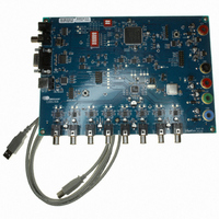
CDB5368
Manufacturer Part Number
CDB5368
Description
BOARD EVAL FOR CS5368 192KHZ ADC
Manufacturer
Cirrus Logic Inc
Specifications of CDB5368
Number Of Adc's
1
Number Of Bits
24
Sampling Rate (per Second)
192k
Data Interface
Serial
Inputs Per Adc
8 Differential
Input Range
±0.3 V
Voltage Supply Source
Analog and Digital
Operating Temperature
-40°C ~ 85°C
Utilized Ic / Part
CS5368
Description/function
Audio A/D
Operating Supply Voltage
3.3 V
Product
Audio Modules
For Use With/related Products
CS5368
Lead Free Status / RoHS Status
Contains lead / RoHS non-compliant
Lead Free Status / RoHS Status
Lead free / RoHS Compliant, Contains lead / RoHS non-compliant
Other names
598-1157


DS624F4
SERIAL AUDIO INTERFACE - I²S/LJ TIMING
The serial audio port is a three-pin interface consisting of SCLK, LRCK and SDOUT.
Logic "0" = GND = 0 V; Logic "1" = VLS; C
Notes:
Sample Rates
Master Mode
SCLK Frequency
SCLK Period
SCLK Duty Cycle
LRCK setup
LRCK hold
SDOUT setup
SDOUT hold
Slave Mode
SCLK Frequency
SCLK Period
SCLK Duty Cycle
LRCK setup
LRCK hold
SDOUT setup
SDOUT hold
1. Duty cycle of generated SCLK depends on duty cycle of received MCLK as specified under
2. CLKMODE functionality described in
3. In Slave Mode, the SCLK/LRCK ratio can be set according to preference. However, chip performance
Clocking” on page
is guaranteed only when using the ratios in
25.
(Note 3)
(Note 1)
SDOUT
SCLK
LRCK
Parameter
before SCLK rising (VLS = 1.8 V)
before SCLK rising (VLS = 3.3 V)
after SCLK rising (VLS = 1.8 V)
after SCLK rising (VLS = 3.3 V)
before SCLK rising (VLS = 5 V)
after SCLK rising (VLS = 1.8 V)
after SCLK rising (VLS = 3.3 V)
after SCLK rising (VLS = 5 V)
after SCLK rising (VLS = 5 V)
10.
(CLKMODE =
(CLKMODE =
data
channel
Double-Speed Mode
Single-Speed Mode
Quad-Speed Mode
before SCLK rising
before SCLK rising
before SCLK rising
t
HOLD1
after SCLK rising
after SCLK rising
1/(64*216 kHz)
1/(64*216 kHz)
L
= 20 pF, timing threshold is 50% of VLS.
0)(Note 2)
1)(Note 2)
Figure 3. I²S/LJ Timing
Section 4.6.3
t
PERIOD
Section 4.7 Master and Slave Clock Frequencies on page
Symbol
t
t
t
t
t
t
t
t
t
t
t
t
t
t
t
t
SETUP1
SETUP2
SETUP1
SETUP2
SETUP2
SETUP2
PERIOD
PERIOD
t
t
t
HOLD1
HOLD2
HOLD2
HOLD2
t
HOLD1
HOLD2
HOLD2
HOLD2
SET UP2
HIGH
HIGH
HIGH
-
-
-
channel
t
SET UP1
"Master Mode Clock Dividers" on page
data
64*Fs
Min
72.3
72.3
108
54
40
28
20
20
10
20
10
28
20
20
10
10
20
10
2
5
4
5
-
t
HOLD2
t
HIGH
64*Fs
Typ
50
33
-
-
-
-
-
-
-
-
-
64*Fs
Max
108
216
54
60
38
65
-
-
-
-
-
-
-
CS5368
24.
“System
Unit
kHz
Hz
Hz
ns
ns
ns
ns
ns
ns
%
%
%
15
Related parts for CDB5368
Image
Part Number
Description
Manufacturer
Datasheet
Request
R

Part Number:
Description:
Development Kit
Manufacturer:
Cirrus Logic Inc
Datasheet:
Part Number:
Description:
Development Kit
Manufacturer:
Cirrus Logic Inc
Datasheet:


Part Number:
Description:
High-efficiency PFC + Fluorescent Lamp Driver Reference Design
Manufacturer:
Cirrus Logic Inc
Datasheet:
Part Number:
Description:
Development Kit
Manufacturer:
Cirrus Logic Inc
Datasheet:
Part Number:
Description:
Development Kit
Manufacturer:
Cirrus Logic Inc
Datasheet:

Part Number:
Description:
Development Kit
Manufacturer:
Cirrus Logic Inc
Datasheet:
Part Number:
Description:
Development Kit
Manufacturer:
Cirrus Logic Inc
Datasheet:
Part Number:
Description:
Development Kit
Manufacturer:
Cirrus Logic Inc
Datasheet:
Part Number:
Description:
Development Kit
Manufacturer:
Cirrus Logic Inc
Datasheet:

Part Number:
Description:
EVALUATION BOARD FOR CS8427
Manufacturer:
Cirrus Logic Inc
Datasheet:

Part Number:
Description:
BOARD EVAL FOR CS8416 RCVR
Manufacturer:
Cirrus Logic Inc
Datasheet:

Part Number:
Description:
EVALUATION BOARD FOR CS8420
Manufacturer:
Cirrus Logic Inc
Datasheet:

Part Number:
Description:
KIT DEVELOPMENT EP9315 ARM9
Manufacturer:
Cirrus Logic Inc
Datasheet:

Part Number:
Description:
KIT DEVELOPMENT EP9302 ARM9
Manufacturer:
Cirrus Logic Inc
Datasheet: