CDB5529 Cirrus Logic Inc, CDB5529 Datasheet - Page 22
CDB5529
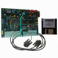
Manufacturer Part Number
CDB5529
Description
EVAL BOARD FOR CS5529
Manufacturer
Cirrus Logic Inc
Specifications of CDB5529
Number Of Adc's
1
Number Of Bits
16
Sampling Rate (per Second)
303
Data Interface
Serial
Inputs Per Adc
2 Differential
Input Range
±2.5 V
Power (typ) @ Conditions
2.6mW @ 2.5 V
Voltage Supply Source
Analog and Digital, Dual ±
Operating Temperature
-40°C ~ 85°C
Utilized Ic / Part
CS5529
Lead Free Status / RoHS Status
Contains lead / RoHS non-compliant
Other names
598-1015


SDO flag falls. For instance, the user can just read
the conversion data register again to exit the contin-
uous conversion mode.
Note:
Output Coding
As shown in the Output Conversion Data Register
Descriptions, the CS5529 presents output conver-
sions as a 24-bit conversion word. The first 16 bits
22
Note: VFS in the table equals the voltage between ground and full scale for any of the unipolar gain ranges,
MSB
D23
D11
3
or the voltage between ± full scale for any of the bipolar gain ranges. See text about error flags under
overrange conditions.
1) If the user begins to clear the SDO flag and
read the conversion data, this action must be
finished before the conversion cycle which is
occurring in the background is complete if the
user wants to be able to read the new
conversion data.
2) If a CC command is issued to the converter
while it is performing a conversion, the filter
will stop the current conversion and start a
new convolution cycle to perform a new
conversion.
3) Continuous conversions aren’t allowed
unless the port flag bit is set in the
configuration register.
4) The converter will remain in data mode and
continually perform conversions until the exit
command is issued (i.e. to exit the user must
read a register).
Unipolar Input Voltage
D22
D10
14
2
>(VFS-1.5 LSB)
VFS/2-0.5 LSB
Table 2. Output Conversion Data Register Description (16 bits + flags).
VFS-1.5 LSB
<(+0.5 LSB)
+0.5 LSB
D21
D9
13
1
LSB
D20
D8
12
Table 3. CS5529 16-bit Output Coding.
D19
D7
11
Offset Binary
1
FFFE
FFFF
FFFF
7FFF
8000
0001
0000
0000
-----
-----
-----
D18
D6
10
1
D17
D5
9
1
of the conversion word represent conversion data.
The third byte contains two error flag bits.
In the third byte, D7-D4 are always logic 1; D3-D2
are always logic 0; and bits D1-D0 are the two flag
bits. The OF (Overrange Flag) bit is set to a logic 1
any time the input signal is: 1) more positive than
positive full scale, 2) more negative than zero (un-
ipolar mode), 3) more negative than negative full
scale (bipolar mode). It is cleared back to logic 0
whenever a conversion word occurs which is not
overranged.The OD (Oscillation Detect) bit is set to
a logic 1 any time that an oscillatory condition is de-
tected in the modulator. This does not occur under
normal operating conditions, but may occur when-
ever the input to the converter is extremely over-
ranged. If the OD bit is set, the conversion data bits
can be completely erroneous. The OD flag bit will be
cleared to logic 0 when the modulator becomes sta-
ble.
Table 2 and Table 3 illustrate the output coding for
the CS5529. Unipolar conversions are output in bi-
nary format and bipolar conversions are output
two's complement.
Bipolar Input Voltage
<(-VFS+0.5 LSB)
>(VFS-1.5 LSB)
-VFS+0.5 LSB
VFS-1.5 LSB
-0.5 LSB
D16
D4
8
1
D15
D3
7
0
D14
Complement
D2
6
0
Two's
7FFF
7FFF
7FFE
FFFF
0000
8001
8000
8000
-----
-----
-----
D13
OD
D1
5
CS5529
DS246F5
D12
OF
D0
4
Related parts for CDB5529
Image
Part Number
Description
Manufacturer
Datasheet
Request
R

Part Number:
Description:
Development Kit
Manufacturer:
Cirrus Logic Inc
Datasheet:
Part Number:
Description:
Development Kit
Manufacturer:
Cirrus Logic Inc
Datasheet:


Part Number:
Description:
High-efficiency PFC + Fluorescent Lamp Driver Reference Design
Manufacturer:
Cirrus Logic Inc
Datasheet:
Part Number:
Description:
Development Kit
Manufacturer:
Cirrus Logic Inc
Datasheet:
Part Number:
Description:
Development Kit
Manufacturer:
Cirrus Logic Inc
Datasheet:

Part Number:
Description:
Development Kit
Manufacturer:
Cirrus Logic Inc
Datasheet:
Part Number:
Description:
Development Kit
Manufacturer:
Cirrus Logic Inc
Datasheet:
Part Number:
Description:
Development Kit
Manufacturer:
Cirrus Logic Inc
Datasheet:
Part Number:
Description:
Development Kit
Manufacturer:
Cirrus Logic Inc
Datasheet:

Part Number:
Description:
EVALUATION BOARD FOR CS8427
Manufacturer:
Cirrus Logic Inc
Datasheet:

Part Number:
Description:
BOARD EVAL FOR CS8416 RCVR
Manufacturer:
Cirrus Logic Inc
Datasheet:

Part Number:
Description:
EVALUATION BOARD FOR CS8420
Manufacturer:
Cirrus Logic Inc
Datasheet:

Part Number:
Description:
KIT DEVELOPMENT EP9315 ARM9
Manufacturer:
Cirrus Logic Inc
Datasheet:

Part Number:
Description:
KIT DEVELOPMENT EP9302 ARM9
Manufacturer:
Cirrus Logic Inc
Datasheet: