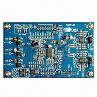
CDB5560 Cirrus Logic Inc, CDB5560 Datasheet - Page 8
CDB5560
Manufacturer Part Number
CDB5560
Description
DEV BOARD FOR CS5560 W/MUX
Manufacturer
Cirrus Logic Inc
Type
A/Dr
Specifications of CDB5560
Number Of Adc's
1
Number Of Bits
24
Sampling Rate (per Second)
50k
Data Interface
Serial
Inputs Per Adc
1 Differential
Input Range
±3 V
Power (typ) @ Conditions
90mW @ 2.5 V
Voltage Supply Source
Dual ±
Operating Temperature
-40°C ~ 85°C
Utilized Ic / Part
CS5560
Product
Data Conversion Development Tools
Conversion Rate
50 KSPS
Resolution
24 bit
Maximum Clock Frequency
16 MHz
Interface Type
SPI
Supply Voltage (max)
3.3 V
Supply Voltage (min)
- 2.5 V
For Use With/related Products
CS5560
Lead Free Status / RoHS Status
Contains lead / RoHS non-compliant
Lead Free Status / RoHS Status
Lead free / RoHS Compliant, Contains lead / RoHS non-compliant
Other names
598-1273
CDB5560-1
CDB5560-1


3.4
3.4.1
The CDB5560 evaluation board hardware comes pre-configured so the only connection required between
it and a data acquisition system is the serial port connection.
The hardware setup is reconfigurable through the hardware control interface connectors. Configure the
evaluation board by setting the appropriate control line to the appropriate logic level.
3.4.2
The CS5560 ADC communications port features an SPI™ serial port. It can be configured for SSC mode
(Master) or SEC mode (Slave) mode as shown in Table 4. Test points are provided to monitor serial com-
munications.
Connections to the serial interface are made according to the following table.
8
Serial Port Communication
Bipolar / Unipolar Mode
Data Conversion Mode
Input Channel Select
Analog Input Buffers
Serial Port Mode
Data Ready Flag
Digital Section
Sleep Mode
Hardware Configuration
Function
SPI™ Serial Port Communications
Reset
Serial Data Output
Serial Data Input
Serial Clock
Chip Select
Function
Continuous Conversion = Active (Low)
Sync. Self Clock = Enabled (High)
Data Ready When Set (Low)
Chip Select = Enabled (Low)
INPUT A = Selected (Low)
Table 4. Hardware Configuration Signals
Buffers = Enabled (High)
Bipolar = Enabled (High)
Reset = Inactive (High)
Sleep = Inactive (High)
Table 5. Serial Interface Connections
Default Level
Label
SCLK
SDO
SDI
CS
Connector
J8, Pin 2
J8, Pin 4
J8, Pin 8
J8, Pin 6
SMODE
BP / UP
BUFEN
SLEEP
CONV
Label
MUX
RDY
RST
CS
J6, Pin 6; S1
Connector
J6, Pin 16
J6, Pin 12
J8, Pin 10
J8, Pin 12
J6, Pin 2
J6, Pin 4
J8, Pin 2
Test Point
J1
E23
E24
E25
E26
CDB5560
Test Point
J3, Pin 2
J3, Pin 3
J3, Pin 8
J3, Pin 9
J3, Pin 4
J3, Pin 6
J3, Pin1
DS713DB4
E23
E21
Related parts for CDB5560
Image
Part Number
Description
Manufacturer
Datasheet
Request
R

Part Number:
Description:
Development Kit
Manufacturer:
Cirrus Logic Inc
Datasheet:
Part Number:
Description:
Development Kit
Manufacturer:
Cirrus Logic Inc
Datasheet:


Part Number:
Description:
High-efficiency PFC + Fluorescent Lamp Driver Reference Design
Manufacturer:
Cirrus Logic Inc
Datasheet:
Part Number:
Description:
Development Kit
Manufacturer:
Cirrus Logic Inc
Datasheet:
Part Number:
Description:
Development Kit
Manufacturer:
Cirrus Logic Inc
Datasheet:

Part Number:
Description:
Development Kit
Manufacturer:
Cirrus Logic Inc
Datasheet:
Part Number:
Description:
Development Kit
Manufacturer:
Cirrus Logic Inc
Datasheet:
Part Number:
Description:
Development Kit
Manufacturer:
Cirrus Logic Inc
Datasheet:
Part Number:
Description:
Development Kit
Manufacturer:
Cirrus Logic Inc
Datasheet:

Part Number:
Description:
EVALUATION BOARD FOR CS8427
Manufacturer:
Cirrus Logic Inc
Datasheet:

Part Number:
Description:
BOARD EVAL FOR CS8416 RCVR
Manufacturer:
Cirrus Logic Inc
Datasheet:

Part Number:
Description:
EVALUATION BOARD FOR CS8420
Manufacturer:
Cirrus Logic Inc
Datasheet:

Part Number:
Description:
KIT DEVELOPMENT EP9315 ARM9
Manufacturer:
Cirrus Logic Inc
Datasheet:

Part Number:
Description:
KIT DEVELOPMENT EP9302 ARM9
Manufacturer:
Cirrus Logic Inc
Datasheet: