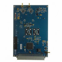
EVAL-AD7685CBZ Analog Devices Inc, EVAL-AD7685CBZ Datasheet - Page 15
EVAL-AD7685CBZ
Manufacturer Part Number
EVAL-AD7685CBZ
Description
BOARD EVAL FOR AD7685
Manufacturer
Analog Devices Inc
Series
PulSAR®r
Specifications of EVAL-AD7685CBZ
Number Of Adc's
1
Number Of Bits
16
Sampling Rate (per Second)
250k
Data Interface
Serial
Inputs Per Adc
1 Differential
Input Range
±VREF
Power (typ) @ Conditions
10mW @ 250kSPS
Voltage Supply Source
Single Supply
Operating Temperature
-40°C ~ 85°C
Utilized Ic / Part
AD7685
Lead Free Status / RoHS Status
Lead free / RoHS Compliant


ANALOG INPUTS
Figure 28 shows an equivalent circuit of the input structure of
the AD7685.
The two diodes, D1 and D2, provide ESD protection for the
analog inputs IN+ and IN−. Care must be taken to ensure that
the analog input signal never exceeds the supply rails by more
than 0.3 V because this will cause these diodes to begin to
forward-bias and start conducting current. These diodes can
handle a forward-biased current of 130 mA maximum. For
instance, these conditions could eventually occur when the
input buffer’s (U1) supplies are different from VDD. In such a
case, an input buffer with a short-circuit current limitation can
be used to protect the part.
This analog input structure allows the sampling of the
differential signal between IN+ and IN−. By using this
differential input, small signals common to both inputs are
rejected, as shown in Figure 29, which represents the typical
CMRR over frequency. For instance, by using IN− to sense a
remote signal ground, ground potential differences between
the sensor and the local ADC ground are eliminated.
OR IN–
80
70
60
50
40
GND
1
IN+
Figure 29. Analog Input CMRR vs. Frequency
Figure 28. Equivalent Analog Input Circuit
10
C
V
V
PIN
DD
DD
= 5V
= 2.5V
VDD
FREQUENCY (kHz)
D1
D2
100
R
1000
IN
C
IN
10000
Rev. B | Page 15 of 28
During the acquisition phase, the impedance of the analog
inputs (IN+ or IN−) can be modeled as a parallel combination
of capacitor C
of R
typically 3 kΩ and is a lumped component made up of some
serial resistors and the on resistance of the switches. C
typically 30 pF and is mainly the ADC sampling capacitor.
During the conversion phase, where the switches are opened,
the input impedance is limited to C
1-pole, low-pass filter that reduces undesirable aliasing effects
and limits the noise.
When the source impedance of the driving circuit is low, the
AD7685 can be driven directly. Large source impedances
significantly affect the ac performance, especially THD. The dc
performances are less sensitive to the input impedance. The
maximum source impedance depends on the amount of THD
that can be tolerated. The THD degrades as a function of the
source impedance and the maximum input frequency, as shown
in Figure 30.
–100
–110
–120
IN
–60
–70
–80
–90
Figure 30. THD vs. Analog Input Frequency and Source Resistance
and C
0
R
R
R
R
S
S
S
S
= 250Ω
= 100Ω
IN
= 50Ω
= 33Ω
PIN
. C
and the network formed by the series connection
PIN
25
is primarily the pin capacitance. R
FREQUENCY (kHz)
50
PIN
. R
IN
and C
75
IN
make a
AD7685
IN
IN
100
is
is
Related parts for EVAL-AD7685CBZ
Image
Part Number
Description
Manufacturer
Datasheet
Request
R


Part Number:
Description:
BOARD EVAL FOR SI270X-A
Manufacturer:
Silicon Laboratories Inc
Datasheet:

Part Number:
Description:
BUCK CONV REF DESIGN KIT IP1201
Manufacturer:
International Rectifier
Datasheet:
Part Number:
Description:
BOARD DEMO SYNC DUAL BUCK CNVTER
Manufacturer:
International Rectifier
Datasheet:
Part Number:
Description:
BOARD DEMO SYNC BUCK CONVETER
Manufacturer:
International Rectifier
Datasheet:

Part Number:
Description:
EVALBOARD/EB Omnidirectional microphone - Analog
Manufacturer:
Analog Devices
Datasheet:
Part Number:
Description:
EVALBOARD/EB Omnidirectional microphone - Analog
Manufacturer:
Analog Devices
Datasheet:


Part Number:
Description:
BOARD EVAL LED DRIVER LT3756
Manufacturer:
Linear Technology
Datasheet:

Part Number:
Description:
BOARD EVAL FOR AD7741/7742
Manufacturer:
Analog Devices Inc
Datasheet:

Part Number:
Description:
±1.7g Dual-Axis IMEMS Accelerometer Evaluation Board
Manufacturer:
Analog Devices Inc
Datasheet:

Part Number:
Description:
IC MULTIPLIER ANALOG 8-SOIC T/R
Manufacturer:
Analog Devices Inc
Datasheet:

Part Number:
Description:
IC ANALOG MULTIPLIER 8-DIP
Manufacturer:
Analog Devices Inc
Datasheet:
Part Number:
Description:
IC ANALOG MULTIPLIER 8-SOIC
Manufacturer:
Analog Devices Inc
Datasheet:
Part Number:
Description:
IC ANALOG MULTIPLIER 8-DIP
Manufacturer:
Analog Devices Inc
Datasheet: