EVAL-AD7767-1EDZ Analog Devices Inc, EVAL-AD7767-1EDZ Datasheet - Page 5
EVAL-AD7767-1EDZ
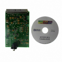
Manufacturer Part Number
EVAL-AD7767-1EDZ
Description
BOARD EVAL AD7767-1 64KSPS 111DB
Manufacturer
Analog Devices Inc
Specifications of EVAL-AD7767-1EDZ
Number Of Adc's
1
Number Of Bits
24
Sampling Rate (per Second)
64k
Data Interface
Serial
Inputs Per Adc
1 Differential
Input Range
±VREF
Power (typ) @ Conditions
10.5mW @ 64kSPS
Voltage Supply Source
Analog and Digital
Operating Temperature
-40°C ~ 105°C
Utilized Ic / Part
AD7767-1
Lead Free Status / RoHS Status
Lead free / RoHS Compliant


TIMING SPECIFICATIONS
AV
unless otherwise noted.
Table 3.
Parameter
DRDY OPERATION
Read OPERATION
Read OPERATION WITH CS LOW
DAISY-CHAIN OPERATION
SYNC/PD OPERATION
1
2
3
Sample tested during initial release to ensure compliance. All input signals are specified with tr = tf = 5 ns (10% to 90% of DV
t
MCLK frequency is 1.024 MHz.
n = 1 for AD7767, n = 2 for the AD7767-1, n = 4 for the AD7767-2.
2
t
t
t
t
t
t
t
t
t
t
t
t
t
t
t
t
t
t
t
t
t
t
t
t
t
and t
DD
1
2
3
4
5
READ
DRDY
6
7
8
9
10
11
SCLK
12
13
14
15
16
17
18
19
20
21
SETTLING
2
2
= DV
3
3
3
allow a ~90% to 10% duty cycle to be used for the MCLK input, where the minimum is 10% for the clock high time and 90% for MCLK low time. The maximum
3
DD
= 2.5 V ± 5%, V
1
DRIVE
= 1.7 V to 3.6 V, V
Limit at t
510
100
900
265
128
71
294
435
492
t
n × 8 × t
0
6
60
50
25
24
10
10
10
1/t
6
0
0
0
1
2
1
20
1
510
(592 × n) + 2
DRDY
8
− t
5
MCLK
MIN
, t
MAX
REF
Unit
ns typ
ns min
ns max
ns typ
ns typ
ns typ
ns typ
ns typ
ns typ
ns typ
ns typ
ns min
ns max
ns max
ns max
ns max
ns max
ns min
ns min
ns min
sec min
ns max
ns min
ns min
ns max
ns min
ns max
ns typ
ns typ
ns min
ns typ
t
= 5 V, common-mode input = V
MCLK
Rev. C | Page 5 of 24
Description
MCLK rising edge to DRDY falling edge
MCLK high pulse width
MCLK low pulse width
MCLK rising edge to DRDY rising edge (AD7767)
MCLK rising edge to DRDY rising edge (AD7767-1)
MCLK rising edge to DRDY rising edge (AD7767-2)
DRDY pulse width (AD7767)
DRDY pulse width (AD7767-1)
DRDY pulse width (AD7767-2)
DRDY low period, read data during this period
DRDY period
DRDY falling edge to CS setup time
CS falling edge to SDO tristate disabled
Data access time after SCLK falling edge (V
Data access time after SCLK falling edge (V
Data access time after SCLK falling edge (V
Data access time after SCLK falling edge (V
SCLK falling edge to data valid hold time (V
SCLK high pulse width
SCLK low pulse width
Minimum SCLK period
Bus relinquish time after CS rising edge
CS rising edge to DRDY rising edge
DRDY falling edge to data valid setup time
DRDY rising edge to data valid hold time
SDI valid to SCLK falling edge setup time
SCLK falling edge to SDI valid hold time
SYNC/PD falling edge to MCLK rising edge
MCLK rising edge to DRDY rising edge going into SYNC/PD mode
SYNC/PD rising edge to MCLK rising edge
MCLK rising edge to DRDY falling edge coming out of SYNC/PD mode
Filter settling time after a reset or power-down
REF
/2, T
A
= −40°C (T
DD
) and timed from a voltage level of 1.7 V.
DRIVE
DRIVE
DRIVE
DRIVE
MIN
DRIVE
) to +105°C (T
= 1.7 V)
= 2.3 V)
= 2.7 V)
= 3.0 V)
= 3.6 V)
AD7767
MAX
),
Related parts for EVAL-AD7767-1EDZ
Image
Part Number
Description
Manufacturer
Datasheet
Request
R

Part Number:
Description:
IC, ADJ LDO REG, 1.5V TO 5V 250mA MSOP-8
Manufacturer:
Vishay
Datasheet:

Part Number:
Description:
IC, ADJ LDO REG, 1.5V TO 5V 0.6A 8-TSSOP
Manufacturer:
Vishay
Datasheet:
Part Number:
Description:
IC, ADJ LDO REG, 1.5V TO 5V 250mA MSOP-8
Manufacturer:
Vishay
Datasheet:

Part Number:
Description:
IC ADJ LDO REG 1.5V TO 5V 150mA 5-SOT-23
Manufacturer:
Vishay
Datasheet:

Part Number:
Description:
BOARD EVAL AS1324-AD
Manufacturer:
austriamicrosystems
Datasheet:
Part Number:
Description:
IC, ADJ LDO REG, 1.5V TO 5V 0.6A 8-TSSOP
Manufacturer:
Vishay
Datasheet:

Part Number:
Description:
IC, ADJ LDO REG, 1.5V TO 5V, 0.3A, MSOP8
Manufacturer:
Vishay
Datasheet:
Part Number:
Description:
IC, ADJ LDO REG, 1.5V TO 5V, 0.3A, MSOP8
Manufacturer:
Vishay
Datasheet:
Part Number:
Description:
IC, ADJ LDO REG 1.215V TO 5V 0.3A MSOP-8
Manufacturer:
Vishay
Datasheet:
Part Number:
Description:
IC, ADJ LDO REG 1.215V TO 5V 0.3A MSOP-8
Manufacturer:
Vishay
Datasheet:

Part Number:
Description:
±1.7g Dual-Axis IMEMS Accelerometer Evaluation Board
Manufacturer:
Analog Devices Inc
Datasheet:

Part Number:
Description:
IC MULTIPLIER ANALOG 8-SOIC T/R
Manufacturer:
Analog Devices Inc
Datasheet:

Part Number:
Description:
IC ANALOG MULTIPLIER 8-DIP
Manufacturer:
Analog Devices Inc
Datasheet:
Part Number:
Description:
IC ANALOG MULTIPLIER 8-SOIC
Manufacturer:
Analog Devices Inc
Datasheet:
Part Number:
Description:
IC ANALOG MULTIPLIER 8-DIP
Manufacturer:
Analog Devices Inc
Datasheet: