CDB5532U Cirrus Logic Inc, CDB5532U Datasheet - Page 12
CDB5532U
Manufacturer Part Number
CDB5532U
Description
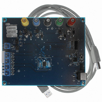
BOARD EVAL FOR CS5532U ADC
Manufacturer
Cirrus Logic Inc
Specifications of CDB5532U
Number Of Adc's
2
Number Of Bits
24
Sampling Rate (per Second)
3.84k
Data Interface
Serial
Inputs Per Adc
1 Differential
Input Range
±2.5 V
Power (typ) @ Conditions
35mW @ 3.84kSPS
Voltage Supply Source
Analog and Digital, Dual ±
Operating Temperature
-40°C ~ 85°C
Utilized Ic / Part
CS5532
Description/function
Audio DSPs
Operating Supply Voltage
5 V
Product
Audio Modules
For Use With/related Products
C8051F320
Lead Free Status / RoHS Status
Contains lead / RoHS non-compliant
Lead Free Status / RoHS Status
Lead free / RoHS Compliant, Contains lead / RoHS non-compliant
Other names
598-1159


2. GENERAL DESCRIPTION
The CS5532/34 are highly integrated ∆Σ Analog-
to-Digital Converters (ADCs) which use charge-
balance techniques to achieve 24-bit performance.
The ADCs are optimized for measuring low-level
unipolar or bipolar signals in weigh scale, process
control, scientific, and medical applications.
To accommodate these applications, the ADCs
come as either two-channel (CS5532) or four-chan-
nel (CS5534) devices and include a very-low-
noise, chopper-stabilized, programmable-gain in-
strumentation amplifier (PGIA, 6 nV/√Hz @
0.1 Hz) with selectable gains of 1×, 2×, 4×, 8×,
16×, 32×, and 64×. These ADCs also include a
fourth-order ∆Σ modulator followed by a digital
filter which provides twenty selectable output word
rates of 6.25, 7.5, 12.5, 15, 25, 30, 50, 60, 100, 120,
200, 240, 400, 480, 800, 960, 1600, 1920, 3200, and
3840 Samples per second (MCLK = 4.9152 MHz).
To ease communication between the ADCs and a
microcontroller, the converters include a simple
three-wire serial interface which is SPI and Mi-
12
AIN4+
AIN1+
AIN2+
AIN1+
AIN4-
AIN1-
AIN2-
AIN1-
*
*
*
CS5531/32 IN+
CS5533/34
M
U
M
U
X
X
IN-
IN+
IN-
IN+
IN-
GAIN is the gain setting of the PGIA (i.e. 2, 4, 8, 16, 32, 64)
Figure 3. Multiplexer Configuration
XGAIN
X1
X1
1000 Ω
1000 Ω
22 nF
X 1
X 1
C1 PIN
C2 PIN
crowire compatible with a Schmitt-trigger input on
the serial clock (SCLK).
2.1. Analog Input
Figure 3 illustrates a block diagram of the
CS5532/34. The front end consists of a multiplexer,
a unity gain coarse/fine charge input buffer, and a
programmable-gain, chopper-stabilized instrumen-
tation amplifier. The unity gain buffer is activated
any time conversions are performed with a gain of
one and the instrumentation amplifier is activated
any time conversions are performed with gain set-
tings greater than one.
The unity gain buffer is designed to accommodate
rail-to-rail input signals. The common mode plus
signal range for the unity gain buffer amplifier is
VA- to VA+. Typical CVF (sampling) current for
the unity gain buffer amplifier is about 50 nA
(MCLK = 4.9152 MHz, see Figure 4).
The instrumentation amplifier is chopper stabilized
and operates with a chop-clock frequency of
MCLK/128. The CVF (sampling) current into the
VREF+
X1
Differential
Modulator
4
th
∆Σ
Order
VREF-
X1
Digital
Filter
Sinc
5
Programmable
Digital Filter
CS5532/34-BS
Sinc
3
DS755F3
Serial
Port
Related parts for CDB5532U
Image
Part Number
Description
Manufacturer
Datasheet
Request
R

Part Number:
Description:
Development Kit
Manufacturer:
Cirrus Logic Inc
Datasheet:
Part Number:
Description:
Development Kit
Manufacturer:
Cirrus Logic Inc
Datasheet:


Part Number:
Description:
High-efficiency PFC + Fluorescent Lamp Driver Reference Design
Manufacturer:
Cirrus Logic Inc
Datasheet:
Part Number:
Description:
Development Kit
Manufacturer:
Cirrus Logic Inc
Datasheet:
Part Number:
Description:
Development Kit
Manufacturer:
Cirrus Logic Inc
Datasheet:

Part Number:
Description:
Development Kit
Manufacturer:
Cirrus Logic Inc
Datasheet:
Part Number:
Description:
Development Kit
Manufacturer:
Cirrus Logic Inc
Datasheet:
Part Number:
Description:
Development Kit
Manufacturer:
Cirrus Logic Inc
Datasheet:
Part Number:
Description:
Development Kit
Manufacturer:
Cirrus Logic Inc
Datasheet:

Part Number:
Description:
EVALUATION BOARD FOR CS8427
Manufacturer:
Cirrus Logic Inc
Datasheet:

Part Number:
Description:
BOARD EVAL FOR CS8416 RCVR
Manufacturer:
Cirrus Logic Inc
Datasheet:

Part Number:
Description:
EVALUATION BOARD FOR CS8420
Manufacturer:
Cirrus Logic Inc
Datasheet:

Part Number:
Description:
KIT DEVELOPMENT EP9315 ARM9
Manufacturer:
Cirrus Logic Inc
Datasheet:

Part Number:
Description:
KIT DEVELOPMENT EP9302 ARM9
Manufacturer:
Cirrus Logic Inc
Datasheet: