CDB5534U Cirrus Logic Inc, CDB5534U Datasheet - Page 2
CDB5534U
Manufacturer Part Number
CDB5534U
Description
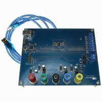
EVAL BOARD FOR CS5534
Manufacturer
Cirrus Logic Inc
Specifications of CDB5534U
Number Of Adc's
1
Number Of Bits
24
Sampling Rate (per Second)
3.84k
Data Interface
Serial
Inputs Per Adc
2 Single
Input Range
0 ~ 2.5 V
Power (typ) @ Conditions
35mW @ 5 V
Voltage Supply Source
Analog and Digital, Dual ±
Operating Temperature
-40°C ~ 85°C
Utilized Ic / Part
CS5534
Description/function
Audio DSPs
Operating Supply Voltage
5 V
Product
Audio Modules
For Use With/related Products
C8051F320
Lead Free Status / RoHS Status
Contains lead / RoHS non-compliant
Lead Free Status / RoHS Status
Lead free / RoHS Compliant, Contains lead / RoHS non-compliant
Other names
598-1016


TABLE OF CONTENTS
2
1. CHARACTERISTICS AND SPECIFICATIONS ..........................................................4
2. GENERAL DESCRIPTION .......................................................................................12
3. PIN DESCRIPTIONS ...............................................................................................44
4. SPECIFICATION DEFINITIONS ...............................................................................46
5. ORDERING INFORMATION .....................................................................................47
6. ENVIRONMENTAL, MANUFACTURING, & HANDLING INFORMATION ..............47
7. PACKAGE DRAWINGS ...........................................................................................48
2.1. Analog Input ....................................................................................................12
2.2. Overview of ADC Register Structure and Operating Modes ............................14
2.3. Configuration Register .....................................................................................23
2.4. Setting up the CSRs for a Measurement .........................................................27
2.5. Calibration ........................................................................................................30
2.6. Performing Conversions ..................................................................................33
2.7. Using Multiple ADCs Synchronously ...............................................................36
2.8. Conversion Output Coding ..............................................................................36
2.9. Digital Filter ......................................................................................................38
2.10. Clock Generator ...............................................................................................39
2.11. Power Supply Arrangements ...........................................................................39
2.12. Getting Started ................................................................................................43
2.13. PCB Layout .....................................................................................................43
ANALOG CHARACTERISTICS..........................................................................4
TYPICAL RMS NOISE (NV), CS5531/32/33/34 .................................................7
TYPICAL NOISE-FREE RESOLUTION(BITS), CS5532/34 ...............................7
5 V DIGITAL CHARACTERISTICS ....................................................................8
3 V DIGITAL CHARACTERISTICS ....................................................................8
DYNAMIC CHARACTERISTICS ........................................................................9
ABSOLUTE MAXIMUM RATINGS .....................................................................9
SWITCHING CHARACTERISTICS ..................................................................10
2.1.1. Analog Input Span .................................................................................... 13
2.1.2. Multiplexed Settling Limitations ............................................................13
2.1.3. Voltage Noise Density Performance .....................................................13
2.1.4. No Offset DAC ......................................................................................14
2.2.1. System Initialization ..............................................................................15
2.2.2. Serial Port Interface ..............................................................................22
2.2.3. Reading/Writing On-Chip Registers ......................................................23
2.3.1. Power Consumption .............................................................................23
2.3.2. System Reset Sequence ......................................................................23
2.3.3. Input Short ............................................................................................24
2.3.4. Guard Signal .........................................................................................24
2.3.5. Voltage Reference Select .....................................................................24
2.3.6. Output Latch Pins .................................................................................24
2.3.7. Offset and Gain Select ..........................................................................25
2.3.8. Filter Rate Select ..................................................................................25
2.5.1. Calibration Registers ............................................................................30
2.5.2. Performing Calibrations ........................................................................31
2.5.3. Self-calibration ......................................................................................31
2.5.4. System Calibration ................................................................................32
2.5.5. Calibration Tips .....................................................................................32
2.5.6. Limitations in Calibration Range ...........................................................33
2.6.1. Single Conversion Mode .......................................................................33
2.6.2. Continuous Conversion Mode ..............................................................34
2.6.3. Examples of Using CSRs to Perform Conversions and Calibrations ....35
CS5531/32/33/34-AS
DS289F5
Related parts for CDB5534U
Image
Part Number
Description
Manufacturer
Datasheet
Request
R

Part Number:
Description:
Development Kit
Manufacturer:
Cirrus Logic Inc
Datasheet:
Part Number:
Description:
Development Kit
Manufacturer:
Cirrus Logic Inc
Datasheet:


Part Number:
Description:
High-efficiency PFC + Fluorescent Lamp Driver Reference Design
Manufacturer:
Cirrus Logic Inc
Datasheet:
Part Number:
Description:
Development Kit
Manufacturer:
Cirrus Logic Inc
Datasheet:
Part Number:
Description:
Development Kit
Manufacturer:
Cirrus Logic Inc
Datasheet:

Part Number:
Description:
Development Kit
Manufacturer:
Cirrus Logic Inc
Datasheet:
Part Number:
Description:
Development Kit
Manufacturer:
Cirrus Logic Inc
Datasheet:
Part Number:
Description:
Development Kit
Manufacturer:
Cirrus Logic Inc
Datasheet:
Part Number:
Description:
Development Kit
Manufacturer:
Cirrus Logic Inc
Datasheet:

Part Number:
Description:
EVALUATION BOARD FOR CS8427
Manufacturer:
Cirrus Logic Inc
Datasheet:

Part Number:
Description:
BOARD EVAL FOR CS8416 RCVR
Manufacturer:
Cirrus Logic Inc
Datasheet:

Part Number:
Description:
EVALUATION BOARD FOR CS8420
Manufacturer:
Cirrus Logic Inc
Datasheet:

Part Number:
Description:
KIT DEVELOPMENT EP9315 ARM9
Manufacturer:
Cirrus Logic Inc
Datasheet:

Part Number:
Description:
KIT DEVELOPMENT EP9302 ARM9
Manufacturer:
Cirrus Logic Inc
Datasheet: